Preparation method of heterogeneous Ge-based pin diode string in reconfigurable multilayer holographic antenna

A technology of diode strings and holographic antennas, applied in antennas, radiation element structures, semiconductor/solid-state device manufacturing, etc., can solve the problems of low carrier mobility, large injection dose and energy, and low integration High carrier mobility, improved breakdown voltage, and improved device performance

Inactive Publication Date: 2017-04-26
XIAN UNIV OF SCI & TECH
View PDF3 Cites 1 Cited by
  • Summary
  • Abstract
  • Description
  • Claims
  • Application Information

AI Technical Summary

Problems solved by technology

[0005] At present, the materials used in pin diodes used in reconfigurable antennas at home and abroad are all bulk silicon materials. This material has the problem of low carrier mobility in the intrinsic region, which affects the carrier concentration in the intrinsic region of the pin diode, which in turn affects Its solid-state plasma concentration; and the P region and N region of this structure are mostly formed by implantation process, which requires a large implant dose and energy, high requirements on equipment, and is not compatible with existing processes; and the use of diffusion process, although The junction depth is deep, but at the same time, the area of ​​the P region and the N region is relatively large, the integration degree is low, and the doping concentration is uneven, which affects the electrical performance of the pin diode, resulting in poor controllability of the solid-state plasma concentration and distribution

Method used


Image

  • Preparation method of heterogeneous Ge-based pin diode string in reconfigurable multilayer holographic antenna
  • Preparation method of heterogeneous Ge-based pin diode string in reconfigurable multilayer holographic antenna
  • Preparation method of heterogeneous Ge-based pin diode string in reconfigurable multilayer holographic antenna

Examples


Embodiment 1

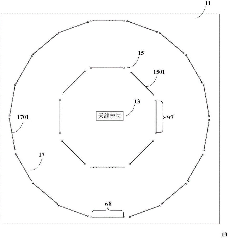
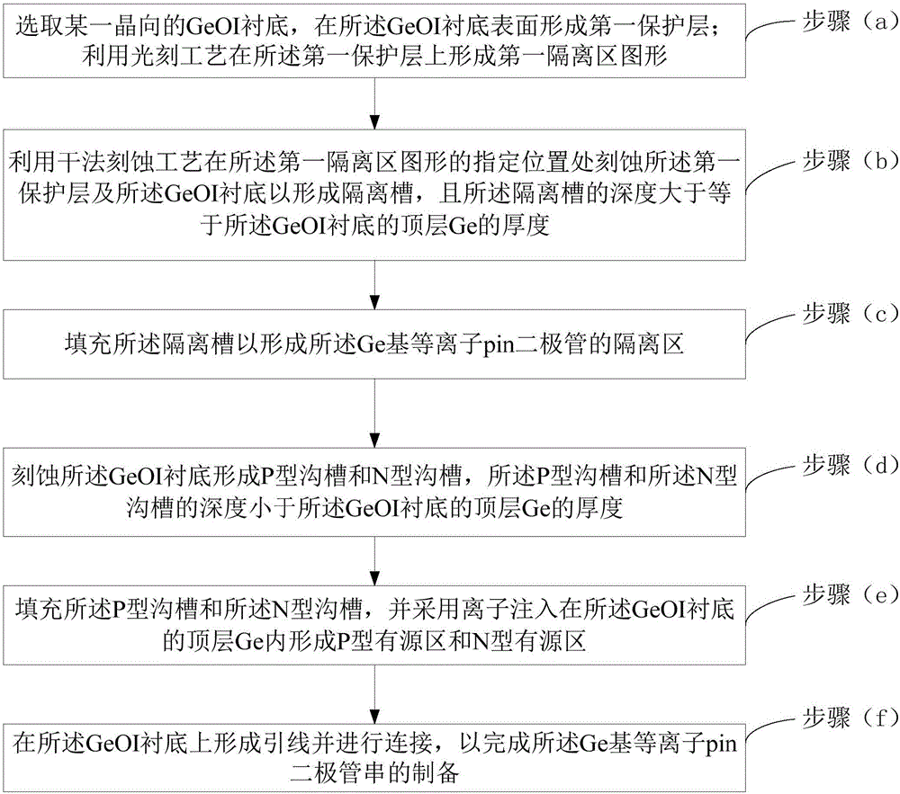
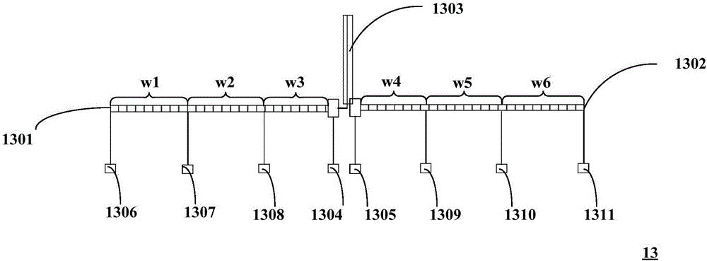
[0062] The embodiment of the present invention provides a method for preparing a heterogeneous Ge-based pin diode string in a reconfigurable multilayer holographic antenna, and the heterogeneous Ge-based plasma pin diode string is used to manufacture a reconfigurable multilayer holographic antenna (1), Please refer to figure 1 , figure 1 This is a schematic structural diagram of a reconfigurable multilayer holographic antenna provided by an embodiment of the present invention; the holographic antenna (1) includes: a semiconductor substrate (11), an antenna module (13), and a first holographic ring (15) And a second holographic ring (17); the antenna module (13), the first holographic ring (15), and the second holographic ring (17) are all fabricated on the semiconductor substrate using a semiconductor process (11) Top; wherein, the antenna module (13), the first holographic ring (15) and the second holographic ring (17) all include pin diode strings connected in series;

[0063] ...

Embodiment 2

[0116] See Figure 8a-Figure 8r , Figure 8a-Figure 8r It is a schematic diagram of another manufacturing method of a heterogeneous Ge-based pin diode for a reconfigurable multilayer holographic antenna provided by an embodiment of the present invention. On the basis of the first embodiment above, a GeOI-based solid-state plasma pin diode with a channel length of 22 nm (the length of the solid plasma region is 100 microns) is taken as an example for detailed description. The specific steps are as follows:

[0117] Step 1, preparation steps of substrate material:

[0118] (1a) such as Figure 8a As shown, the (100) crystal orientation is selected, the doping type is p-type, and the GeOI substrate 101 with a doping concentration of 1014cm-3, and the thickness of the top layer Ge is 50μm;

[0119] (1b) such as Figure 8b As shown, a first SiO2 layer 201 with a thickness of 40 nm is deposited on a GeOI substrate by using a chemical vapor deposition (CVD) method;

[0120] (1c) Using a chem...

Embodiment 3

[0147] Please refer to Picture 9 , Picture 9 It is a schematic diagram of another device structure of a heterogeneous Ge-based plasma pin diode provided by an embodiment of the present invention. The heterogeneous Ge-based plasma pin diode adopts the above-mentioned figure 2 The manufacturing method shown is produced. Specifically, the Ge-based plasma pin diode is prepared and formed on the GeOI substrate 301, and the P region 304, the N region 305 and the P region 304 and the N region 305 of the pin diode are laterally located between the P region 304 and the N region 305 The intermediate I regions are all located in the top Ge302 of the GeOI substrate. The pin diode can be isolated by STI deep trench isolation, that is, an isolation trench 303 is provided outside the P region 304 and the N region 305, and the depth of the isolation trench 303 is greater than or equal to the thickness of the top layer Ge302.


PUM


Abstract

The invention relates to a preparation method of a heterogeneous Ge-based pin diode string in a reconfigurable multilayer holographic antenna. The preparation method comprises the steps of: selecting a GeOI substrate in a crystal orientation, and setting an isolation region in the GeOI substrate; etching the GeOI substrate to form P-type grooves and N-type grooves, wherein the depth of the P-type grooves and the N-type grooves is less than the thickness of top layer Ge of the GeOI substrate; filling the P-type grooves and the N-type grooves, and adopting ion implantation to form a P-type active region and an N-type active region in the top layer Ge of the GeOI substrate; and forming a lead wire on the GeOI substrate, so as to complete the preparation of the heterogeneous Ge-based pin diodes. The preparation method provided by the invention can prepare and provide high-performance Ge-based plasma pin diodes suitable for forming a solid-state plasma antenna by utilizing the deep trench isolation technology and the ion implantation process.

Description

Technical field [0001] The invention relates to the technical field of semiconductor device manufacturing, in particular to a method for preparing a heterogeneous Ge-based pin diode string in a reconfigurable multilayer holographic antenna. Background technique [0002] A wireless communication system that can dynamically adapt to changing environmental propagation characteristics will be the key to next-generation communication applications. The antenna is an extremely important component in any wireless device because it transmits and receives radio waves. The performance of the antenna represents the performance of most wireless devices, so the performance of the antenna is a key part of the system. [0003] A reconfigurable antenna is an antenna that changes its radiation, polarization and frequency characteristics by changing its physical structure. Among them, frequency reconfigurable antennas have greatly expanded the scope of application because they can be applied to mult...

Claims


Application Information

Patent Timeline
Patent Type & Authority Applications(China)
IPC IPC(8): H01L21/329H01L29/868H01Q1/36H01Q23/00
CPCH01L29/66136H01L29/868H01Q1/36H01Q23/00
Inventor 李妤晨
Owner XIAN UNIV OF SCI & TECH
Why Eureka
Try Eureka