A kind of semiconductor device and its preparation method, electronic device

A technology of electronic devices and semiconductors, applied in semiconductor/solid-state device manufacturing, circuits, electrical components, etc., can solve problems such as increased loss, increased epitaxial resistance, and reduced performance of FinFET devices

Active Publication Date: 2019-09-03
SEMICON MFG INT (SHANGHAI) CORP +1
View PDF4 Cites 0 Cited by
  • Summary
  • Abstract
  • Description
  • Claims
  • Application Information

AI Technical Summary

Problems solved by technology

[0004] During the manufacturing process of FinFET devices, the raised source and drain are usually formed on the source and drain regions by epitaxy to introduce stress in the channel, and at the same time reduce the source and drain epitaxial resistance and contact resistance. There are high temperature processes such as H 2 Pre-baking, etc., the temperature can reach 780-850 ° C, at the higher temperature, the loss of pocket implanted ions in FinFET devices will increase, especially for the loss of B ions in PMOS. This increases the epitaxial resistance and degrades the performance of FinFET devices
Due to the continuous shrinking of the size of semiconductor devices, such as narrower fins, this further exacerbates the loss of B ions and the shadow effect of pocket implants.

Method used


Image

  • A kind of semiconductor device and its preparation method, electronic device
  • A kind of semiconductor device and its preparation method, electronic device
  • A kind of semiconductor device and its preparation method, electronic device

Examples


Embodiment 1

[0039] Combine below Figures 1a-1j , figure 2 The semiconductor device and the preparation method of the present invention are further described.

[0040] Step 201 is executed to provide a semiconductor substrate 101 and perform ion implantation to form a well.

[0041]In this step, the semiconductor substrate 101 may be at least one of the materials mentioned below: silicon, silicon-on-insulator (SOI), silicon-on-insulator (SSOI), silicon-germanium-on-insulator (S- SiGeOI), silicon germanium on insulator (SiGeOI) and germanium on insulator (GeOI), etc.

[0042] Wherein the semiconductor substrate includes an NMOS region and a PMOS region, so as to form NMOS devices and PMOS devices in subsequent steps.

[0043] Next, a pad oxide layer (Pad oxide) is formed on the semiconductor substrate 101, wherein the formation method of the pad oxide layer (Pad oxide) can be formed by a deposition method, such as chemical vapor deposition, atomic layer deposition, etc. , can also be f...

Embodiment 2

[0099] The present invention also provides a semiconductor device, including a semiconductor substrate 101 and a well.

[0100] The semiconductor substrate 101 may be at least one of the materials mentioned below: silicon, silicon-on-insulator (SOI), silicon-on-insulator (SSOI), silicon-germanium-on-insulator (S-SiGeOI), insulator Silicon germanium-on-insulator (SiGeOI) and germanium-on-insulator (GeOI), etc.

[0101] Wherein the semiconductor substrate includes an NMOS area and a PMOS area to form an NMOS device and a PMOS device.

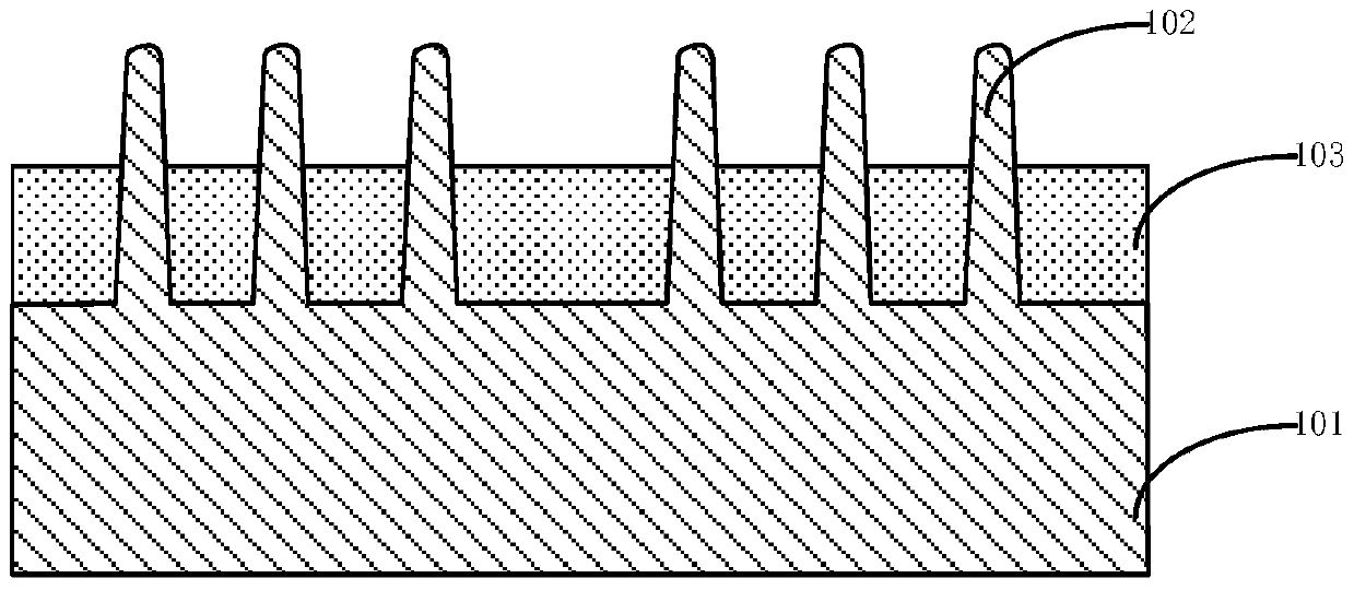
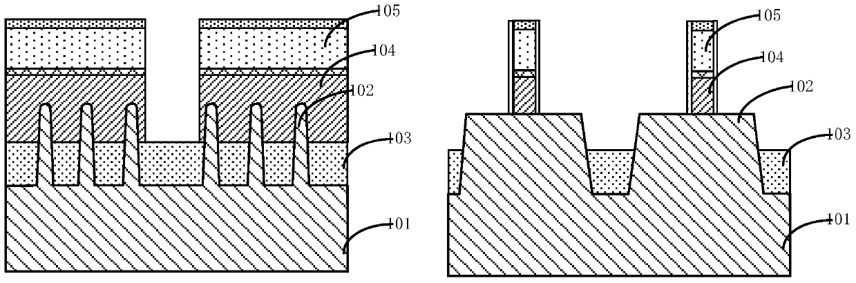
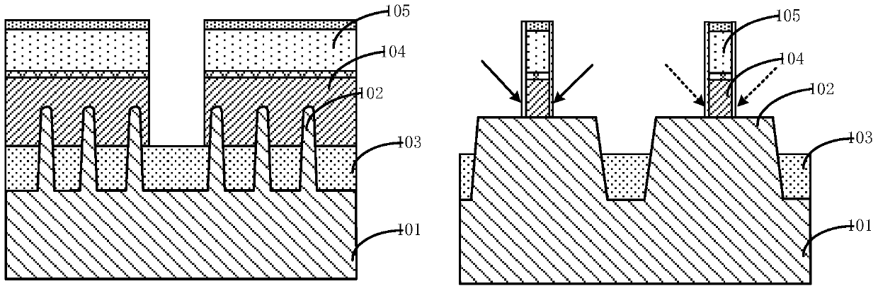
[0102] A plurality of fins 102 are formed on the semiconductor substrate 101, and the widths of the fins are all the same, or the fins are divided into a plurality of fin groups with different widths.

[0103] An isolation material layer 103 is formed between the fins and partially covers the fin structure.

[0104] A gate structure surrounding the fin is formed on the isolation material layer, and the gate structure includes an NMOS gate struct...

Embodiment 3

[0115] The present invention also provides an electronic device, including the semiconductor device described in the second embodiment. Wherein, the semiconductor device is the semiconductor device described in the second embodiment, or the semiconductor device obtained according to the preparation method described in the first embodiment.

[0116] The electronic device of this embodiment can be any electronic product or equipment such as mobile phone, tablet computer, notebook computer, netbook, game console, TV set, VCD, DVD, navigator, camera, video recorder, voice recorder, MP3, MP4, PSP, etc. , can also be any intermediate product including the semiconductor device. The electronic device according to the embodiment of the present invention has better performance due to the use of the above-mentioned semiconductor device.


PUM


Abstract

The invention relates to a semiconductor device, a manufacturing method thereof, and an electronic device. The manufacturing method comprises the step of: S1, providing a semiconductor substrate, and forming a plurality of fins on the semiconductor substrate, wherein the semiconductor substrate comprises an NMOS region and a PMOS region, NMOS gates surrounding the fins are formed on the NMOS region, and PMOS gates surrounding the fins are formed on the PMOS region; S2, executing pocket ion implantation on two sides of the NMOS gates; S3, executing LDD ion implantation on two sides of the NMOS gates, so as to form an NMOS LDD region; S4, forming first grooves on two sides of the PMOS gates and carrying out pre-baking; S5, forming a first semiconductor material layer in each first groove through epitaxial growth, and conducting in-situ doping to form PMOS uplift source-drains; S6, and executing an annealing step so that in-situ doped ions diffuse below the PMOS gates to form a PMOS LDD extension area.

Description

technical field [0001] The present invention relates to the field of semiconductors, in particular, the present invention relates to a semiconductor device, a preparation method thereof, and an electronic device. Background technique [0002] With the continuous development of semiconductor technology, the improvement of integrated circuit performance is mainly achieved by continuously shrinking the size of integrated circuit devices to increase its speed. Currently, as the semiconductor industry has advanced to nanotechnology process nodes in pursuit of high device density, high performance, and low cost, the fabrication of semiconductor devices is limited by various physical limits. [0003] As the dimensions of CMOS devices continue to shrink, manufacturing and design challenges have prompted the development of three-dimensional designs such as Fin Field Effect Transistors (FinFETs). Compared with the existing planar transistors, FinFET is an advanced semiconductor devic...

Claims


Application Information

Patent Timeline
Patent Type & Authority Patents(China)
IPC IPC(8): H01L21/8238
Inventor 周飞
Owner SEMICON MFG INT (SHANGHAI) CORP
Why Eureka
Try Eureka