Thin film transistor and manufacturing method thereof

A technology of thin film transistors and manufacturing methods, applied in the direction of transistors, semiconductor/solid-state device manufacturing, electric solid-state devices, etc., can solve the problems of complex film structure and large off-state current of thin-film transistors, simplify the process, ensure electrical performance, The effect of reducing the off-state current

Inactive Publication Date: 2017-04-26
BOE TECH GRP CO LTD +1
View PDF2 Cites 12 Cited by
  • Summary
  • Abstract
  • Description
  • Claims
  • Application Information

AI Technical Summary

Problems solved by technology

[0004] Embodiments of the present invention provide a method for manufacturing a thin film transistor and a thin film transistor, which are used to solve the problems i

Method used


Image

  • Thin film transistor and manufacturing method thereof
  • Thin film transistor and manufacturing method thereof
  • Thin film transistor and manufacturing method thereof

Examples


Embodiment Construction

[0031] The manufacturing method of the thin film transistor provided by the embodiment of the present invention and the specific implementation manner of the thin film transistor will be described in detail below with reference to the accompanying drawings.

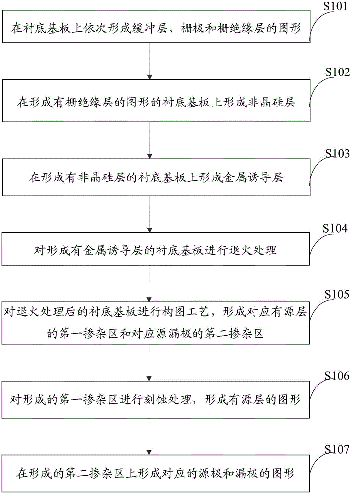
[0032] An embodiment of the present invention provides a method for manufacturing a thin film transistor, such as figure 2 As shown, can include:

[0033] S101, sequentially forming patterns of a buffer layer, a gate, and a gate insulating layer on the base substrate;

[0034] S102, forming an amorphous silicon layer on the base substrate with a pattern of a gate insulating layer;

[0035] S103, forming a metal induction layer on the base substrate formed with the amorphous silicon layer;

[0036] S104, performing annealing treatment on the base substrate formed with the metal induction layer;

[0037] S105. Perform a patterning process on the annealed substrate to form a first doped region corresponding to the active...


PUM


Abstract

The invention discloses a thin film transistor and a manufacturing method thereof. Through carrying out annealing treatment on a substrate on which a metal induced layer is formed, metal induced crystallization can be realized for preparing a bottom gate type low-temperature polycrystalline silicon thin film transistor, and a light shield layer adopted in the manufacturing of a top gate type thin film transistor is omitted, thereby saving the manufacturing cost, simplifying the process, and omitting the polycrystalline silicon doping step through metal induced crystallization. In addition, amorphous silicon is converted into the polycrystalline silicon through metal induced crystallization, and the polycrystalline silicon undergoes a composition process to form a first doped region corresponding to an active layer and a second doped region corresponding to a source-drain region, thereby realizing partition of a channel region and the a source-drain region, and ensuring the electrical performance of the thin film transistor. Furthermore, residual metal particles in the channel region due to metal induced crystallization can be removed through etching the first doped region, an off-state current of the device is decreased, the problem of metal particle residual is solved, and the good electrical performance of the device is ensured.

Description

technical field [0001] The invention relates to the field of display technology, in particular to a manufacturing method of a thin film transistor and the thin film transistor. Background technique [0002] Currently, display devices such as liquid crystal display panels (LCD, Liquid Crystal Display), electroluminescence (EL, electroluminescence) display panels, and electronic paper are well known. These display devices have a thin film transistor (TFT, Thin Film Transistor) that controls the switching of each pixel. Generally, such as figure 1 As shown, the structure of the thin film transistor mainly includes: a light-shielding layer 1, a buffer layer 2, an active layer 3, a gate insulating layer 4, a gate 5, a source 6 and a drain 7 located on a substrate; wherein, the active The layer is made of polysilicon material, and the light-shielding layer is used to block the influence of external light on the polysilicon material, prevent the active layer from generating photo...

Claims


Application Information

Patent Timeline
IPC IPC(8): H01L29/786H01L21/02H01L21/336
CPCH01L21/02532H01L21/02672H01L29/66757H01L29/78675H01L29/78618H01L29/78633H01L27/127H01L27/1277H01L29/78603H01L29/66765H01L21/02592H01L29/78678H01L21/32051H01L21/30604H01L21/2855H01L29/458H01L21/324
Inventor 马明超樊君李付强
Owner BOE TECH GRP CO LTD
Why Eureka
Try Eureka