Preparation method of adopting pulsed laser sputtering deposition of fishing net SiOx film on negative current collector material
A technology of laser sputtering and current collectors, which is applied in the field of lithium-ion batteries, can solve the problems of weak binding force between active materials and current collectors and uneven distribution of active materials, so as to avoid adverse effects on electrochemical performance, easy operation and high efficiency. The effect of specific capacity
- Summary
- Abstract
- Description
- Claims
- Application Information
AI Technical Summary
Problems solved by technology
Method used
Image
Examples
Embodiment 1
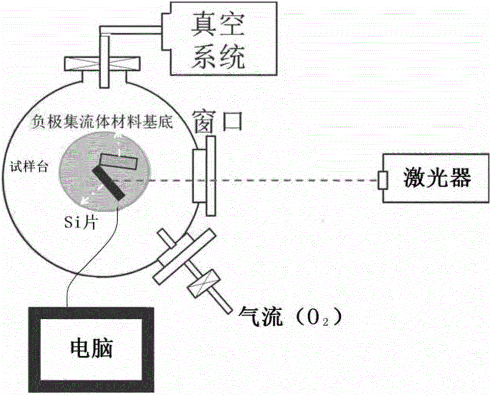
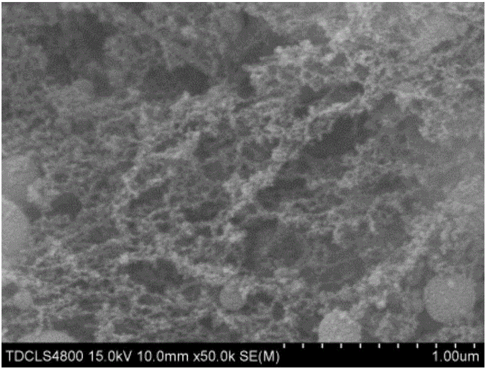
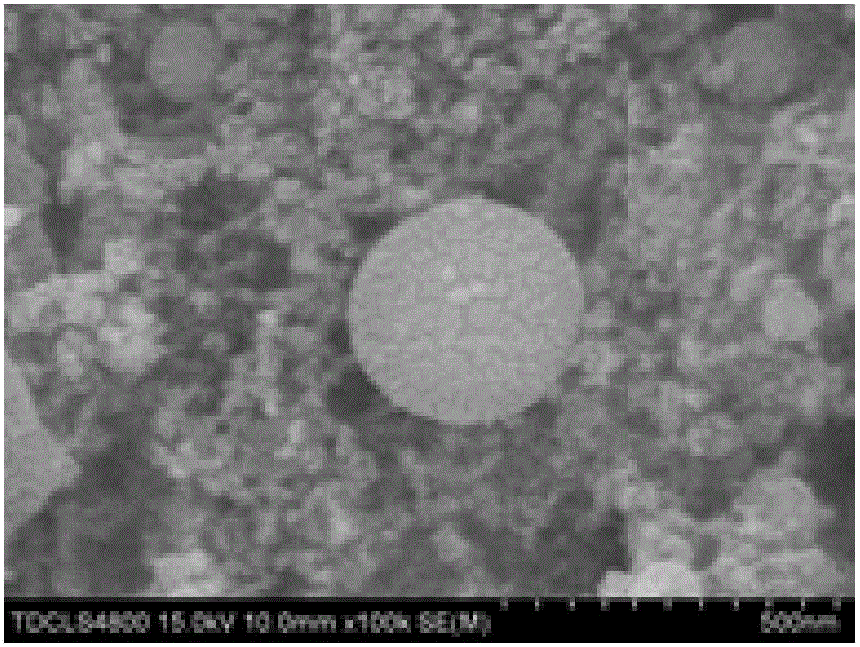
[0018] Embodiment 1: the preparation of the Cu foil of the SiOx film deposited with the network texture structure supported by micron-scale particles, the steps are:
[0019] Step 1. Clean the silicon wafer in acetone, deionized water, and ethanol ultrasonic baths for 10 minutes respectively; use the silicon wafer as the target material and the Cu foil as the substrate, and fix the Cu foil substrate and the silicon wafer on the sample stage at the same time , adjusting the angle between the silicon wafer and the Cu foil substrate to be 60°, and the incident direction of the laser is within the range of ±5° of the bisector of the angle between the silicon wafer and the Cu foil substrate;
[0020] Step 2. Close the vacuum chamber and evacuate to 1×10 4 After Pa, the flow rate of oxygen is 2L / min, which is used as background gas to participate in the reaction, and the vacuum degree is 1×10 during laser sputtering. -2 Pa;
[0021] Step 3. Adjust the laser pulse width of the puls...
Embodiment 2
[0023] Embodiment 2: the preparation of the foamed Fe of the SiO film that is deposited with the network texture structure supported by micron-scale particles, the steps are:
[0024] Step 1. Clean the silicon wafer in acetone, deionized water, and ethanol ultrasonic bath for 10 minutes respectively; use the silicon wafer as the target material, and use the foamed Fe as the substrate, and fix the foamed Fe substrate and the silicon wafer on the sample stage at the same time , adjusting the angle between the silicon wafer and the foamed Fe substrate to be 40°, and the incident direction of the laser is within the range of ±5° of the angle bisector between the silicon wafer and the foamed Fe substrate;
[0025] Step 2. Close the vacuum chamber and evacuate to 1×10 5 After Pa, the flow rate of oxygen is 1L / min, which is used as background gas to participate in the reaction, and the vacuum degree during laser sputtering is 1×10 -3 Pa;
[0026] Step 3. Adjust the laser pulse widt...
Embodiment 3
[0027] Embodiment 3: the preparation of the foamed Ni of the SiOx film that is deposited with the network texture structure supported by micron-scale particles, the steps are:
[0028] Step 1. Clean the silicon wafer in acetone, deionized water and ethanol ultrasonic bath for 10 minutes respectively; use the silicon wafer as the target material and foam Ni as the substrate, and fix the foam Ni substrate and the silicon wafer on the sample stage at the same time , adjust the angle between the silicon wafer and the foamed Ni substrate to be 80°, and the incident direction of the laser is within the range of ±5° of the angle bisector between the silicon wafer and the foamed Ni substrate;
[0029] Step 2. Close the vacuum chamber and evacuate to 5×10 4 After Pa, the flow rate of oxygen is 0.5L / min, which is used as background gas to participate in the reaction, and the vacuum degree during laser sputtering is 5×10 -3 Pa;
[0030] Step 3. Adjust the laser pulse width of the pulse...
PUM
| Property | Measurement | Unit |
|---|---|---|
| Energy density | aaaaa | aaaaa |
Abstract
Description
Claims
Application Information
 - R&D Engineer
- R&D Manager
- IP Professional
- Industry Leading Data Capabilities
- Powerful AI technology
- Patent DNA Extraction
Browse by: Latest US Patents, China's latest patents, Technical Efficacy Thesaurus, Application Domain, Technology Topic, Popular Technical Reports.
© 2024 PatSnap. All rights reserved.Legal|Privacy policy|Modern Slavery Act Transparency Statement|Sitemap|About US| Contact US: help@patsnap.com


