Preparation method of small-period array structure

A technology with an array structure and a small period, which is applied in the photoplate making process of the pattern surface, photomechanical equipment, microlithography exposure equipment, etc., can solve the problem of slow speed, expensive extreme ultraviolet exposure equipment, and can not meet the needs of scientific research and processing and other issues to achieve the effect of high precision and flexible preparation methods

Inactive Publication Date: 2017-05-10
INST OF PHYSICS - CHINESE ACAD OF SCI
View PDF3 Cites 5 Cited by
  • Summary
  • Abstract
  • Description
  • Claims
  • Application Information

AI Technical Summary

Problems solved by technology

Although these approaches can greatly reduce the feature size of devices or structures, there are also some problems in these methods, such as the electron beam lithography process is too slow in the preparation of small periodic arrays, and the extreme ultraviolet exposure equipment is relatively expensive, etc.
With the continuous expansion of the demand for small-period structures, the above processes can no longer meet the needs of scientific research and processing.

Method used


Image

  • Preparation method of small-period array structure
  • Preparation method of small-period array structure
  • Preparation method of small-period array structure

Examples


Embodiment Construction

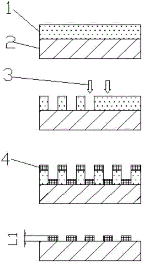
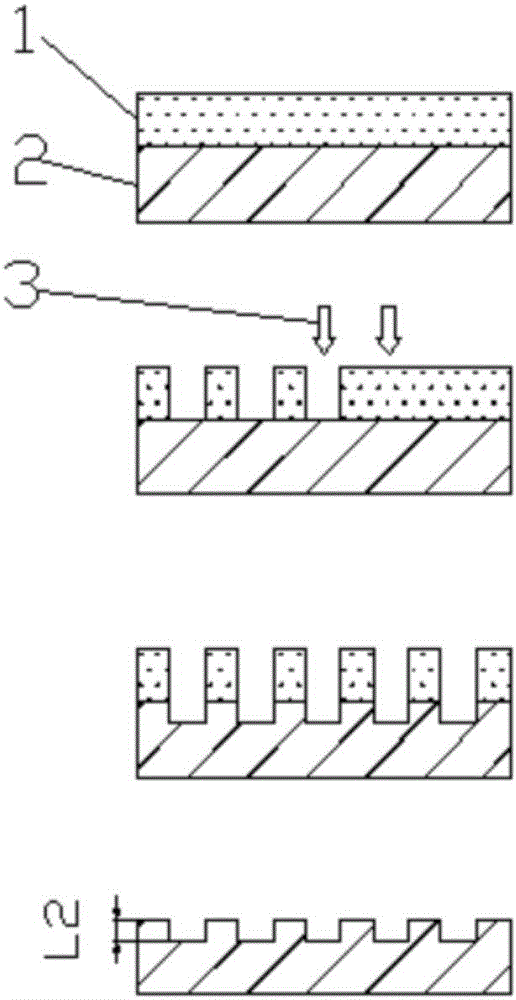
[0034] figure 1 It is a flowchart of a method for preparing a small-period array structure according to an embodiment of the present invention. Such as figure 1 As shown, a preparation method of a small periodic array structure, comprising:

[0035] Step 1: Spin-coat photoresist 1 on substrate 2 .

[0036] The substrate 2 used in step 1 can be a silicon substrate, a silicon dioxide substrate or a sapphire substrate, or a silicon nitride film, a silicon dioxide film or a silicon carbide film grown on the silicon substrate substrate, Any flat substrate with thin-film material that is processed on a flat surface is also possible.

[0037] The photoresist 1 used in step 1 is positive or negative. After the photoresist is exposed to light, it can react quickly in the exposure area, so that the physical properties of this material, especially the solubility and affinity, will change significantly. After being treated with an appropriate solvent, the soluble part will be dissolve...


PUM


Abstract

The invention discloses a preparation method of a small-period array structure and relates to the technical field of two-dimensional micro-nano devices. The preparation method is used for preparing the small-period array structure on a substrate, and comprises the following steps: step 1, spin-coating photoresist on the substrate; step 2, scanning an exposed pattern on the photoresist through adopting an electron beam photoetching process, so as to obtain a photoresist pattern, wherein an exposed step length of the electron beam photoetching process is a large step length so as to guarantee that the photoresist between two electron beam spots is not exposed; step 3, transferring the photoresist pattern onto the substrate, so as to obtain a sample; step 4, putting the sample into photoresist removing liquid to obtain the small-period array structure on the substrate. By adopting the preparation method disclosed by the invention, the step length and dosage of electron beam exposure are controlled, and a small-period array pattern is formed on an electron beam exposure region in a process of scanning on the large-area pattern; the preparation method has the characteristics of rapidness in preparation, good controllability, low cost, capability of preparing in a large area and the like.

Description

technical field [0001] The invention relates to the technical field of two-dimensional micro-nano devices, in particular to a method for preparing a small-period nano-array structure Background technique [0002] With the development of electronic devices and optical devices, nano-array structures with small periods have been increasingly used in the devices used. For example, in optical materials, the response frequency of optical metamaterials is directly related to the linearity and period of the metamaterial structure used. The higher the response frequency of optical metamaterials, the smaller the corresponding metamaterial linearity and period. If metamaterials in the visible light band are to be obtained, the structural period needs to be controlled below 500 nanometers. When making electronic devices, smaller electronic devices provide a higher degree of integration. Moreover, the current requirements for integration are getting higher and higher. There are various...

Claims


Application Information

Patent Timeline
Patent Type & Authority Applications(China)
IPC IPC(8): G03F7/20B82Y40/00
CPCG03F7/2051B82Y40/00G03F7/203
Inventor 顾长志潘如豪李俊杰刘哲唐成春杨海方
Owner INST OF PHYSICS - CHINESE ACAD OF SCI
Why Eureka
Try Eureka