Top emission quantum-dot light-emitting diode (QLED) field-effect transistor with micro-cavity structure and fabrication method of top emission QLED filed-effect transistor

A field-effect transistor and top-emission technology, which is applied in the fields of organic semiconductor devices, semiconductor/solid-state device manufacturing, electric solid-state devices, etc. Monochromaticity and vertical luminous efficiency, achieving selectivity and structural improvement effects

Inactive Publication Date: 2017-05-10
TCL CORPORATION
View PDF10 Cites 13 Cited by
  • Summary
  • Abstract
  • Description
  • Claims
  • Application Information

AI Technical Summary

Problems solved by technology

[0005] In view of the above-mentioned deficiencies in the prior art, the purpose of the present invention is to provide a top-emitting QLED field-effect transistor with a microcavity structure

Method used


Image

  • Top emission quantum-dot light-emitting diode (QLED) field-effect transistor with micro-cavity structure and fabrication method of top emission QLED filed-effect transistor
  • Top emission quantum-dot light-emitting diode (QLED) field-effect transistor with micro-cavity structure and fabrication method of top emission QLED filed-effect transistor
  • Top emission quantum-dot light-emitting diode (QLED) field-effect transistor with micro-cavity structure and fabrication method of top emission QLED filed-effect transistor

Examples


preparation example Construction

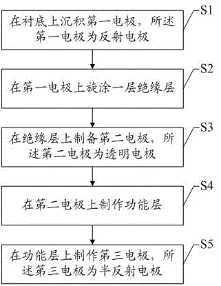
[0042] The present invention also provides a preferred embodiment of the method for preparing a top-emitting QLED field-effect transistor with a microcavity structure as described above, such as figure 2 As shown, it includes the steps:

[0043] S1. Depositing a first electrode on a substrate, where the first electrode is a reflective electrode;

[0044] S2. Spin coating an insulating layer on the first electrode;

[0045] S3. Prepare a second electrode on the insulating layer, and the second electrode is a transparent electrode;

[0046] S4, making a functional layer on the second electrode;

[0047] S5, making a third electrode on the functional layer, the third electrode is a semi-reflective electrode

[0048] In the above step S1, the first electrode 11 is firstly deposited on the substrate 10 by evaporation as the FET gate, and at the same time as the FET anode or FET cathode, and the first electrode 11 is selected from a reflective material with better effect, such a...

Embodiment 1

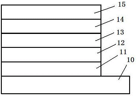
[0055] Such as image 3 As shown, the silicon-based substrate 20 can be cleaned by the standard Shiraki method, using organic solvent ambient ultrasonic, multi-step strong acid treatment, etc. to remove the surface oxide layer, organic impurities and metal element impurities. The first electrode 21 is deposited on the silicon-based substrate 20 by evaporation as the FET gate and as the FET cathode. The first electrode 21 is selected from a good light reflection material, such as Ag or Al, etc., and the thickness is preferably 1-100 nm. For example 20nm.

[0056] An insulating layer 22 is spin-coated on the first electrode 21, and the insulating layer 22 is also used as a device microcavity length adjustment layer, and the thickness of the insulating layer 22 depends on the light-emitting wavelength of the quantum dot light-emitting layer used. The insulating layer 22 is a transparent dielectric material. The insulating layer 22 can be made of PMMA or polyimide (PI). For exam...

Embodiment 2

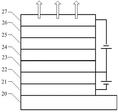
[0063] Such as Figure 4 As shown, the silicon-based substrate 30 can be cleaned by the standard Shiraki method, using organic solvent ambient ultrasonic, multi-step strong acid treatment, etc. to remove the surface oxide layer, organic impurities and metal element impurities. The first electrode 31 is deposited on the silicon-based substrate 30 by evaporation as the gate of the FET and as the anode of the FET. The first electrode 31 is made of a good light-reflecting material, such as Ag or Al, with a thickness of preferably 1-100 nm.

[0064] An insulating layer 32 is spin-coated on the first electrode 31, and the insulating layer 32 also serves as a device microcavity length adjustment layer, and the thickness of the insulating layer 32 depends on the emission wavelength of the quantum dot light-emitting layer used. The insulating layer 32 is a transparent dielectric material. The insulating layer 32 can be made of PMMA or polyimide (PI). For example, when choosing PI mate...


PUM

PropertyMeasurementUnit
Thicknessaaaaaaaaaa
Thicknessaaaaaaaaaa
Thicknessaaaaaaaaaa

Abstract

The invention discloses a top emission quantum-dot light-emitting diode (QLED) field-effect transistor with micro-cavity structure and a fabrication method of the top emission QLED filed-effect transistor. The top emission QLED field-effect transistor comprises a substrate, a first electrode, an insulation layer, a second electrode, a functional layer and a third electrode, wherein the first electrode is a reflection electrode, the second electrode is a transparent electrode, and the third electrode is a half-reflection electrode. Structure improvement and optimization are performed on the electrodes of top emission QLED field-effect transistor, an optical micro-cavity is formed in the device; and by means of an interference effect, light selection is achieved, the monochromaticity of emergent light wavelength corresponding to the cavity length of the optical micro-cavity and the luminous efficiency of a vertical direction are improved.

Description

technical field [0001] The invention relates to the display field, in particular to a top-emitting QLED field-effect transistor with a microcavity structure and a preparation method. Background technique [0002] In recent years, quantum dot light-emitting diodes (QLEDs) have attracted extensive attention and research in the fields of lighting and display due to their many advantages such as high brightness, low power consumption, wide color gamut, and easy processing. In addition, in the context of the development of microelectronics technology, field effect transistors (FETs) are currently one of the most widely used devices in modern microelectronics. Combining the technology of light-emitting devices and FETs, it can be considered to integrate QLEDs and FETs into QLED-FET (QLED Field Effect Transistor) light-emitting devices, so as to make full use of the huge application prospects of QLEDs. [0003] With the maturity of small size and passive driving technology, large ...

Claims


Application Information

Patent Timeline
IPC IPC(8): H01L51/50H01L51/52H01L51/56
CPCH10K50/115H10K50/81H10K50/85H10K2102/3026H10K71/00
Inventor 辛征航向超宇李乐张滔张东华
Owner TCL CORPORATION
Why Eureka
Try Eureka