Miniaturized broadband slow-wave half-mode substrate-integrated waveguide coupler and design method thereof

A half-mode substrate integration and coupler technology, which is applied in the field of couplers, can solve the problems that the conduction characteristics cannot be adjusted twice, the coupling structure of the coupler is single, and the design freedom is low, so as to achieve the controllable phase velocity of the guided wave, good Coupling performance, the effect of controllable operating frequency

Inactive Publication Date: 2017-05-10
UNIV OF ELECTRONIC SCI & TECH OF CHINA
View PDF2 Cites 10 Cited by
  • Summary
  • Abstract
  • Description
  • Claims
  • Application Information

AI Technical Summary

Problems solved by technology

[0007] 2. For SIW-based transmission lines, the conduction characteristics such as cut-off frequency and propagation phase velocity are only related to the substrate material and SIW equivalent width
Once the substrate material selection and waveguide size are limited, its conduction characteristics cannot be adjusted twice, and the design freedom is low
[0008]

Method used


Image

  • Miniaturized broadband slow-wave half-mode substrate-integrated waveguide coupler and design method thereof
  • Miniaturized broadband slow-wave half-mode substrate-integrated waveguide coupler and design method thereof
  • Miniaturized broadband slow-wave half-mode substrate-integrated waveguide coupler and design method thereof

Examples


Example Embodiment

[0037] Example 1

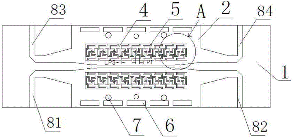
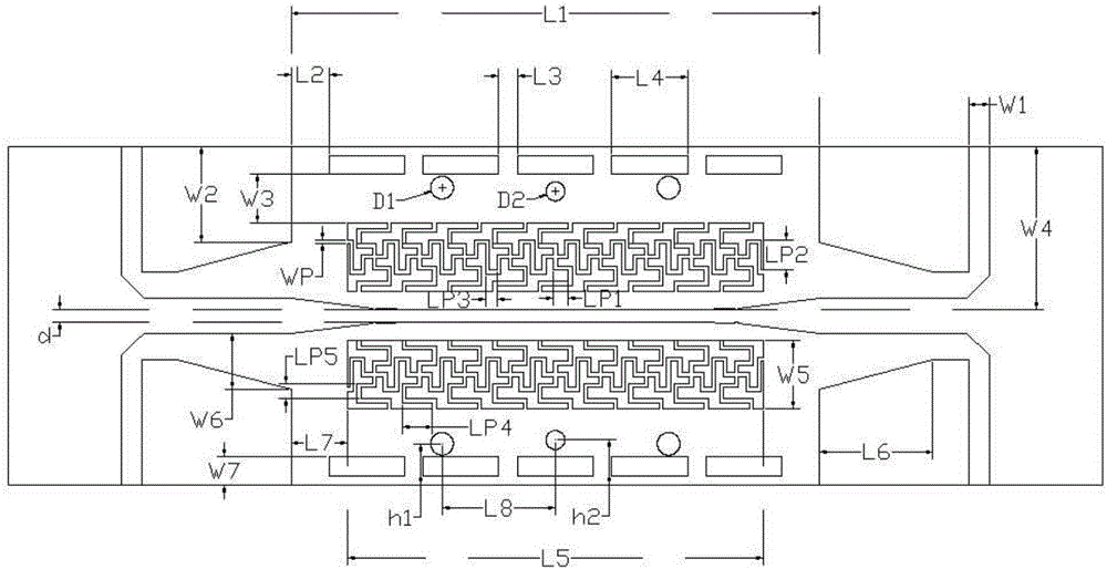
[0038] The slow-wave half-mode substrate integrated waveguide coupler is the SW-HMSIW coupler. like figure 1 The shown miniaturized broadband slow-wave semi-mode substrate integrated waveguide coupler includes a dielectric substrate 1, the upper and lower surfaces of the dielectric substrate 1 are metal cladding layers, and the entire lower surface of the metal cladding layer on the lower surface is used as a ground plane. , the upper surface is processed and etched by the printed circuit board process, and the shape is two half-mode substrate integrated waveguide transmission lines 2 that are symmetrical and non-contact with each other. The inner side of the half-mode substrate integrated waveguide transmission line 2 is opened with a loading window 4, and the loading window 4 passes through The PCB is etched into a microstrip multi-segment line network 5, and the microstrip multi-segment line network 5 forms a hollow pattern structure; the outer side of t...

Example Embodiment

[0039] Example 2

[0040] In this embodiment, the structures of the microstrip polyline network 5 and the loading window 4 are optimized on the basis of the above-mentioned embodiment.

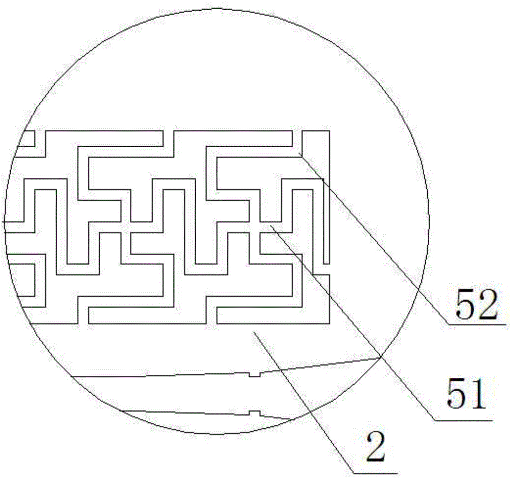
[0041] The loading window 4 is rectangular. The microstrip polyline network 5 includes a plurality of cross-shaped microstrip nodes 51 arranged in sequence along the rectangular loading window, that is, a single-row structure is formed in the lateral direction. The port is connected with a vertical microstrip polyline; the horizontal microstrip polyline realizes the connection between two adjacent microstrip nodes 51 and the microstrip nodes 51 at both ends are connected with the half-mode substrate integrated waveguide transmission line 2; the vertical microstrip The polyline is connected between the microstrip node 51 and the half-mode substrate integrated waveguide transmission line 2, and the microstrip polyline network 5, the transverse microstrip polyline and the longitudinal microstrip...

Example Embodiment

[0044] Example 3

[0045] This embodiment is further improved on the basis of the above-mentioned embodiment, that is, there are multiple metallized through holes 7, the metallized through-holes 7 are arranged in a row along the loading window 4, and the metallized through-hole 7 in the center has the smallest diameter and The diameter gradually increases along the two ends of the connection, and parameters such as the number and diameter of through holes can be replaced by different design requirements.

[0046] The electrical wall can use an existing array of metallized through holes, or can use metallized through grooves.

[0047] The coupler includes an input end 81 , a straight-through output end 82 , a coupling output end 84 and an isolation end 83 . The two ends of the half-mode substrate-integrated waveguide transmission line 2 are respectively connected to the input end 81 and the straight-through output end 82 through the trapezoidal microstrip transition section, a...


PUM

PropertyMeasurementUnit
Thicknessaaaaaaaaaa

Abstract

The invention discloses a miniaturized broadband slow-wave half-mode substrate-integrated waveguide coupler and a design method thereof. An open edge of a half-mode substrate-integrated waveguide transmission line is utilized as a coupling part of the coupler and a microstrip multistage line network is formed by etching on the surface to replace a novel coupler structure formed by a traditional metal surface. Compared with a traditional substrate-integrated waveguide coupler, the miniaturized broadband slow-wave half-mode substrate-integrated waveguide coupler has the advantages that a slow wave effect is formed by introducing a microstrip multistage line into an inductive load, so that the physical size of a coupling edge is effectively reduced; the coupling characteristic of the coupler can be sensitively affected by a multi-parameter adjustable microstrip multistage line structure and the coupling coefficient and the coupling bandwidth can be more flexibly and effectively controlled; meanwhile, a new design freedom is provided for optimization of various performance indexes of the coupler by multiple parameters with adjustable structure sizes in the microstrip multistage line; and compared with a traditional substrate-integrated waveguide coupler, the formed novel coupler has a lower profile, a larger working bandwidth and better coupling performance.

Description

technical field [0001] The invention relates to the field of couplers, in particular to a miniaturized broadband slow-wave half-mode substrate integrated waveguide coupler and a design method thereof. Background technique [0002] In recent years, with the rapid development of microwave and millimeter wave communication systems, substrate integrated waveguide (SIW) technology has attracted widespread attention due to its low cost and complete planar circuit structure. As a new type of planar waveguide structure, the substrate integrated waveguide not only has the characteristics of low loss, high power capacity, and adaptability to high-frequency frequency bands of the traditional metal rectangular waveguide, but also overcomes the characteristics of the traditional waveguide structure, which is too large and difficult to process. The structure miniaturization and easy processing and integration are realized. [0003] The substrate-integrated waveguide is a waveguide struct...

Claims


Application Information

Patent Timeline
IPC IPC(8): H01P5/18H01P11/00
CPCH01P5/184H01P11/00
Inventor 金海焱周瑜亮金海陆黄永茂廖丹
Owner UNIV OF ELECTRONIC SCI & TECH OF CHINA
Why Eureka
Try Eureka