Hermetic chip on board

Active Publication Date: 2020-11-10
RAYTHEON CO
View PDF12 Cites 5 Cited by
  • Summary
  • Abstract
  • Description
  • Claims
  • Application Information

AI Technical Summary

Benefits of technology

[0004]Embodiments of the low permeability, nanolaminate coated film comprise inclusion of a copper layer for use in multilayer printed circuit boards and other applications. The nanolaminate layer can be applied before or after the nanolaminate coated, low permeability polymer film is attached to a conventional high permeability multilayer printed circuit board assembly constructed of inorganic fillers and high permeability resins such as epoxy-based resins. Inclusion of the nanolaminate layer within a free standing, metallized low permeability homogeneous polymer film eliminates the need for application of the nanolaminate coating and selective patterning of the nanolaminate film at the board fabricator or circuit board assembly facility. The low permeability free standing nanolaminate film can then be fabricated cost effectively in batch coating systems and in higher class clean room conditions.
[0005]Further embodiments employ hermetic electronic, optical or electro-mechanical architectures utilizing the metallized, nanolaminate coated, low permeability homogeneous polymer film lamina

Problems solved by technology

Such packages are inherently expensive, and require significantly more size, weight and cost than would be required by directly mounting the active components to the circuit board.
Additionally, the prepackaged devices increase the electrical loss and thermal impedance of the assembled devices.
Plastic encapsulated devices are also inherently more moisture sensitive and can subject the semiconductor devices to dielectric loading effects that degrade device performance and reliability.
For flip chip devices, dielectric loading from flip chip underfill or aerogel can be a major source of degraded output power due to increased internode capacitance.
Prior attempts to achieve a hermetic board assembly using polymeric based materials do not recognize or embody the design features, construction and material properties of the board laminate and coating required to achieve a hermetic level of environmen

Method used


Image

  • Hermetic chip on board
  • Hermetic chip on board
  • Hermetic chip on board

Examples


Embodiment Construction

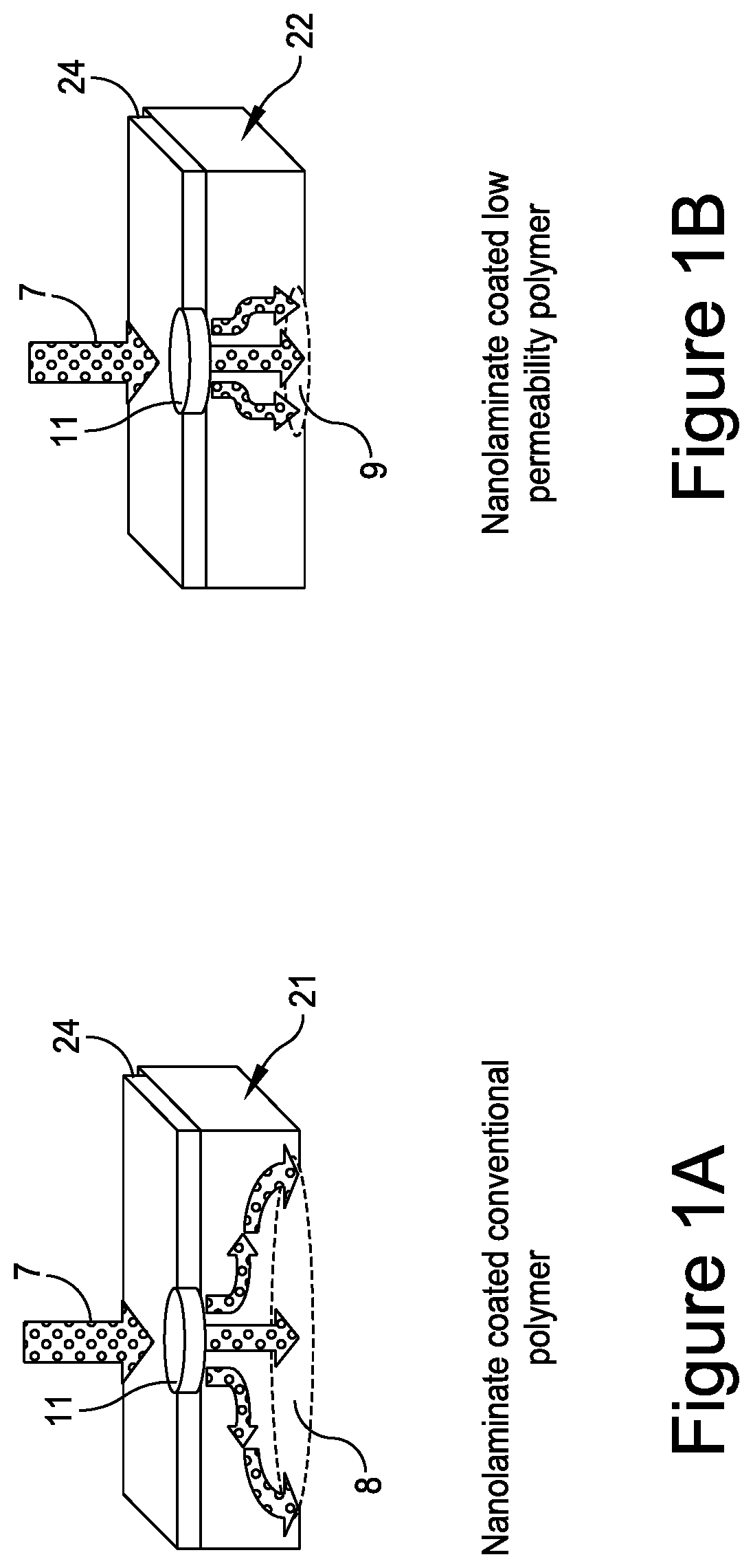
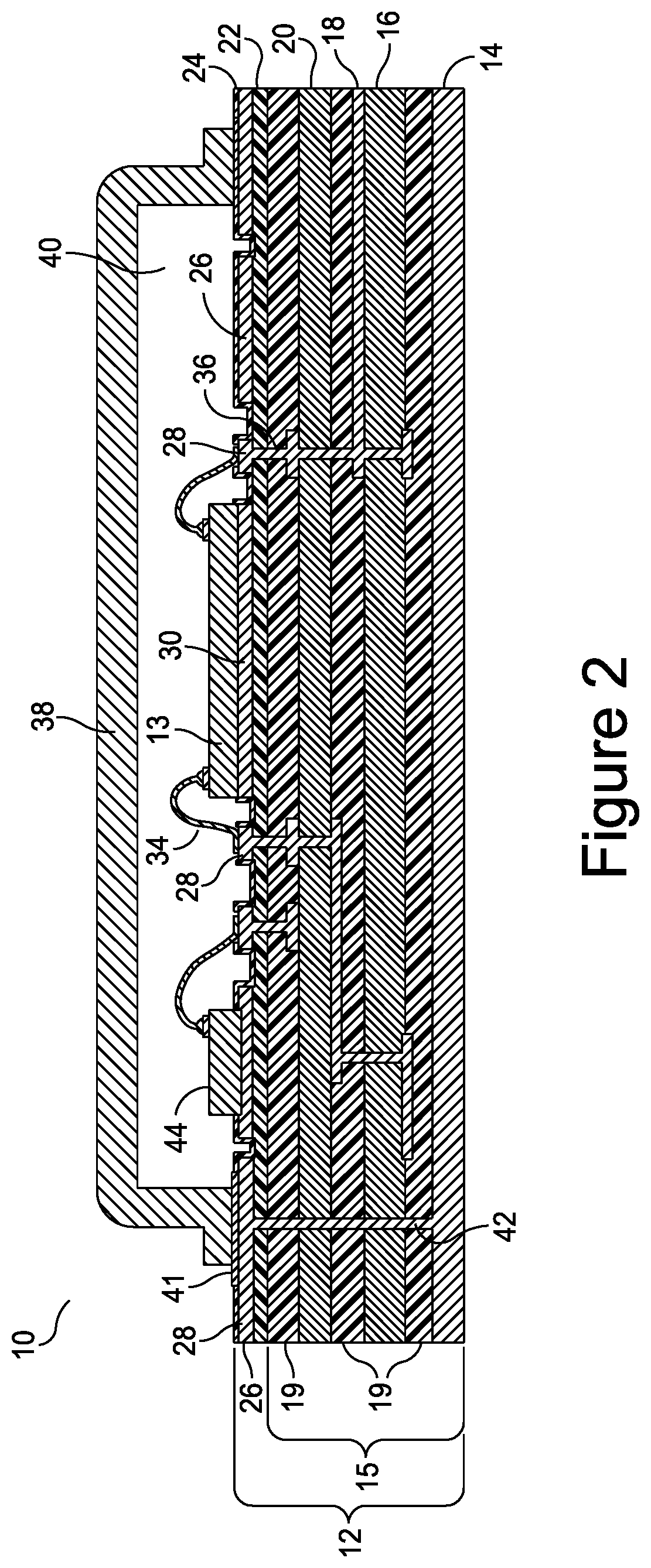
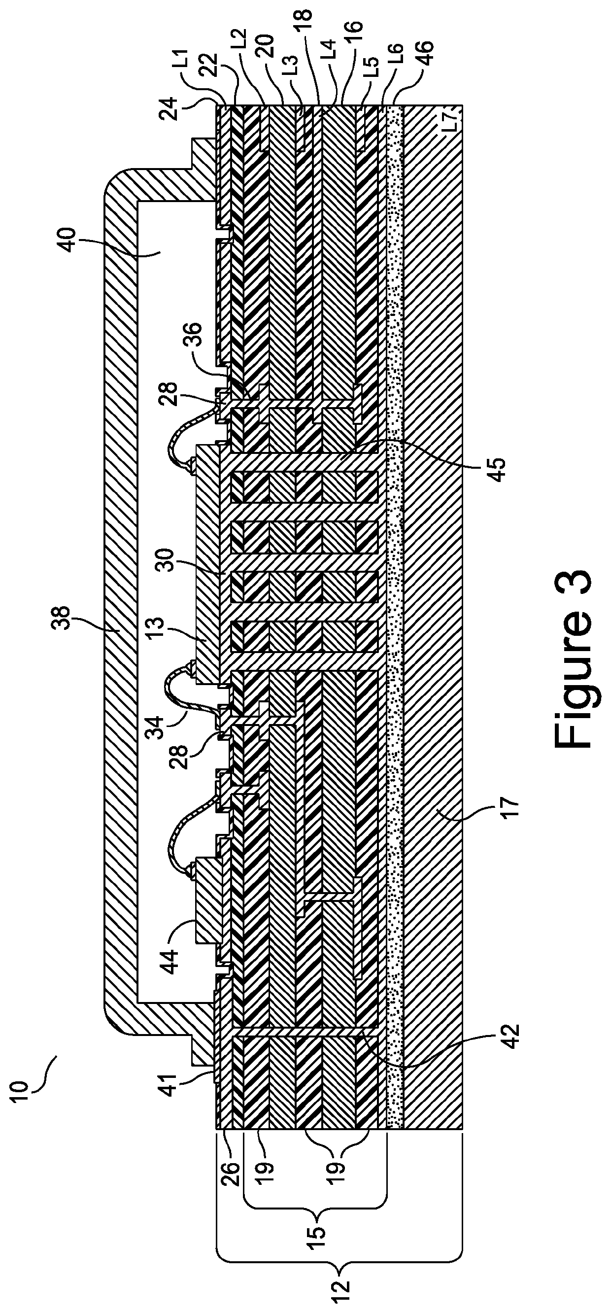
[0042]To realize the requisite low permeation rate required for meeting Military and Industry Standards with a hermetic chip on board architecture, a thin low permeability polymer top or cap layer free of glass, ceramic or other fillers is fabricated separately or as part of the multilayer board structure coated with a much lower permeability nanolaminate inorganic layer. The unfilled low permeability polymer cap layer eliminates physical and material discontinuities in the nanolaminate coating induced by glass weave and or particles in the board and separation from the particles and resin matrix which can occur in elevated temperature processing, thermal cycling and humidity exposure and provides a smooth uniform surface for coating. The low permeability of the cap layer significantly reduces the permeability degradation caused by pinholes, surface particles or other defects in the nanolaminate coating of the cap layer. The low permeability polymer film is selected from a group of ...


PUM


Abstract

A low permeability laminate film includes one or more low moisture permeability homogeneous polymer films with a total thickness between 0.5 and ten mils without glass or ceramic fillers and with a moisture permeability measured at 37° C. and 100% RH of less than 2.6 E-05 atm·cc·mm/in2·sec of air. The polymer film includes one of polychlorotrifluoroethylene, polytetrafluorethylene, fluorinated ethylene propylene, and perfluoro alkoxy alkane. The low permeability laminate film further includes a nanolaminate including alternate combinations of nanolaminate material that is selected from the group consisting of alumina, titanium dioxide, zirconium oxide, beryllium oxide, hafnium oxide, titanium oxide, silicon nitride, tantalum nitride, silica, parylene F, parylene AF-4, parylene HT® and PTFE (polytetrafluoroethylene). A resulting coated nanolaminate film has a moisture permeability less than an equivalent standard leak rate per square inch of 3.0 E-08 atm·cc/in2·sec of air.

Description

BACKGROUND OF THE DISCLOSURE[0001]This disclosure relates generally to mounting electronic components onto a substrate or circuit board, and more particularly, to a circuit board construction and an associated environmental protection system and method of manufacturing the same.[0002]Present day microelectronic assemblies utilize printed circuit boards with active and passive components attached to the circuit board in hermetically sealed and / or plastic encapsulated packages. The hermetic or plastic encapsulated packages are required to environmentally protect the active components from moisture and other adverse materials. Such packages are inherently expensive, and require significantly more size, weight and cost than would be required by directly mounting the active components to the circuit board. Additionally, the prepackaged devices increase the electrical loss and thermal impedance of the assembled devices. Plastic encapsulated devices are also inherently more moisture sensit...

Claims


Application Information

Patent Timeline
IPC IPC(8): H01L23/48H05K1/09H05K1/11H05K1/18H05K3/22H05K3/40H05K1/02H05K3/30H05K3/46H05K3/00
CPCH05K1/0204H05K3/303H05K1/183H05K1/112H05K3/4644H05K3/0035H05K1/09H05K1/181H05K3/22H05K3/4038H05K3/0047H05K2201/10121H05K2201/10083H05K2201/10522H05K2201/10287H05K2201/09509H05K2203/107H01L23/49894H01L23/49822H01L23/36H01L23/13H01L23/10H01L21/50H01L23/053H01L2224/73265H01L2224/48091H01L2224/48227H01L2224/48465H01L2924/16152H10K50/844H01L2924/00014
Inventor BEDINGER, JOHN M.
Owner RAYTHEON CO
Why Eureka
Try Eureka