Preparation method of OLED (Organic Light-Emitting Diode) pixel unit and OLED display panel

A technology for pixel units and display panels, applied in electrical components, semiconductor/solid-state device manufacturing, electric-solid-state devices, etc., can solve the problems affecting the service life of OLED devices, low light extraction efficiency, loss, etc., to avoid internal total reflection, The effect of improving the light output efficiency and improving the service life

Inactive Publication Date: 2017-05-17
EVERDISPLAY OPTRONICS (SHANGHAI) CO LTD
View PDF5 Cites 10 Cited by
  • Summary
  • Abstract
  • Description
  • Claims
  • Application Information

AI Technical Summary

Problems solved by technology

Depending on the formula, adjusting the type of organic molecules in the organic light-emitting layer 3' can produce three primary colors of red, green, and blue to form the basic color, and the brightness or intensity of the light is proportional to the current (the greater the current, the greater the brightness or intensity of the light. The higher the higher), but the existing OLED device, because the OLED device emits light as a ...

Method used


Image

  • Preparation method of OLED (Organic Light-Emitting Diode) pixel unit and OLED display panel
  • Preparation method of OLED (Organic Light-Emitting Diode) pixel unit and OLED display panel
  • Preparation method of OLED (Organic Light-Emitting Diode) pixel unit and OLED display panel

Examples


Embodiment Construction

[0044] The present invention will be further described below in conjunction with the accompanying drawings and specific embodiments, but not as a limitation of the present invention.

[0045] The following will clearly and completely describe the technical solutions in the embodiments of the present invention with reference to the accompanying drawings in the embodiments of the present invention. Obviously, the described embodiments are only some, not all, embodiments of the present invention. Based on the embodiments of the present invention, all other embodiments obtained by persons of ordinary skill in the art without creative efforts fall within the protection scope of the present invention.

[0046] It should be noted that, in the case of no conflict, the embodiments of the present invention and the features in the embodiments can be combined with each other.

[0047] The present invention will be further described below in conjunction with the accompanying drawings and s...


PUM


Abstract

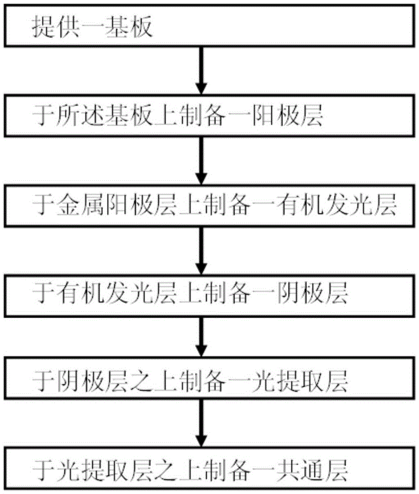
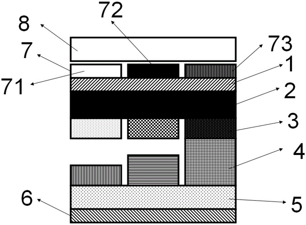
The invention relates to the technical field of semiconductor manufacturing, and particularly relates to a preparation method of an OLED (Organic Light-Emitting Diode) device and an OLED display panel. The preparation method of the OLED device comprises the steps of providing a substrate; preparing an anode layer on the substrate; preparing an organic light-emitting layer on the metal anode layer; preparing a cathode layer on the organic light-emitting layer; and preparing a light extraction layer used for extracting different colors of light-emitting materials on the cathode layer, wherein a refractive index of the cathode layer is lower than a refractive index of the light extraction layer. The refractive index of the cathode layer is lower than the refractive index of the light extraction layer, so that extraction can be performed on 80% of light lost inside the OLED device, total internal reflection of partial light in the transmission process is avoided, and the luminous efficiency of the OLED device is greatly improved.

Description

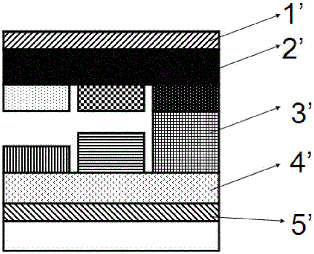
technical field [0001] The invention relates to the technical field of semiconductor manufacturing, in particular to a method for preparing an OLED pixel unit and an OLED display panel. Background technique [0002] Existing OLED (Organic Light-Emitting Diode) devices, such as figure 1 As shown, a schematic structural diagram of an existing OLED device, an anode 5', a hole injection and transport layer 4', an organic light-emitting layer 3', an electron transport and injection layer 2', and a cathode 1 are sequentially arranged on a glass substrate. ', forming a parallel reflective structure. During the use of the OLED device, a voltage is applied between the anode 5' and the cathode 1', and the current flows from the cathode 1' to the anode 5' and passes through the organic light-emitting layer 3' (the current refers to the electron flow), the cathode 1' outputs electrons to the organic light-emitting layer 3', and the anode 5' absorbs electrons from the organic light-emit...

Claims


Application Information

Patent Timeline
IPC IPC(8): H01L51/56H01L51/52
CPCH10K50/858H10K71/00
Inventor 李贵芳肖玲张斌张磊
Owner EVERDISPLAY OPTRONICS (SHANGHAI) CO LTD
Why Eureka
Try Eureka