LED vertical chip structure and manufacturing method thereof

A technology of chip structure and manufacturing method, applied in semiconductor devices, electrical components, circuits, etc., can solve problems affecting chip reliability, leakage, splashing of metal layers, etc., so as to reduce the risk of leakage, avoid metal splashing, and improve reliability. sexual effect

Active Publication Date: 2017-05-24
ENRAYTEK OPTOELECTRONICS
View PDF5 Cites 9 Cited by
  • Summary
  • Abstract
  • Description
  • Claims
  • Application Information

AI Technical Summary

Problems solved by technology

[0008] In view of the above-mentioned shortcomings of the prior art, the purpose of the present invention is to provide a LED vertical chip structure and its manufacturing method, which is used to solve the problem of dry-processing the chip dicing line after the substrate is peele

Method used


Image

  • LED vertical chip structure and manufacturing method thereof
  • LED vertical chip structure and manufacturing method thereof
  • LED vertical chip structure and manufacturing method thereof

Examples


Embodiment 1

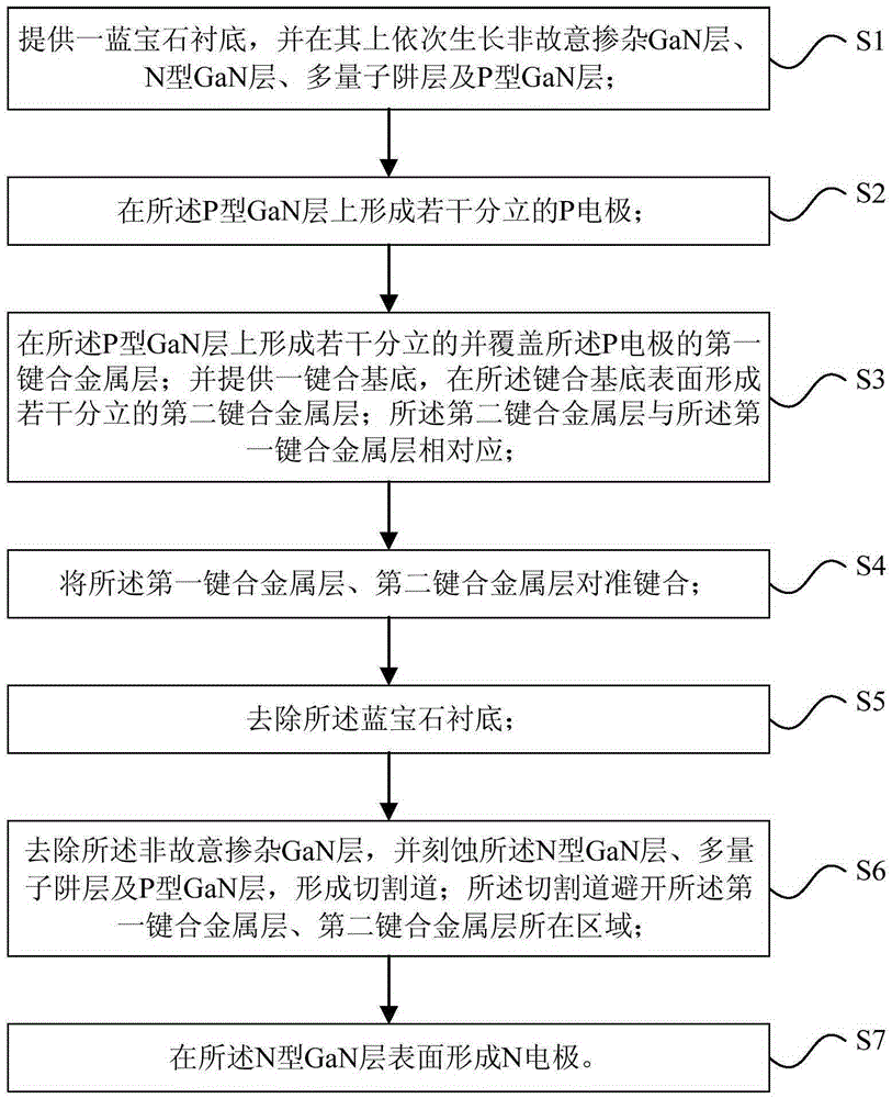
[0063] The present invention provides a method for manufacturing an LED vertical chip structure, please refer to figure 2 , shown as a process flow diagram of the method, comprising the following steps:

[0064] S1: Provide a sapphire substrate, and sequentially grow an unintentionally doped GaN layer, an N-type GaN layer, a multi-quantum well layer and a P-type GaN layer on it;

[0065] S2: forming several discrete P electrodes on the P-type GaN layer;

[0066] S3: forming several discrete first bonding metal layers on the P-type GaN layer and covering the P electrode; and providing a bonding substrate, forming several discrete second bonding layers on the surface of the bonding substrate a metal layer; the second bonding metal layer corresponds to the first bonding metal layer;

[0067] S4: Align and bond the first bonding metal layer and the second bonding metal layer;

[0068] S5: removing the sapphire substrate;

[0069] S6: removing the unintentionally doped GaN lay...

Embodiment 2

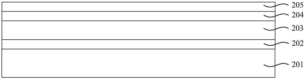
[0094] The present invention also provides a LED vertical chip structure, such as Figure 12 As shown, the chip structure includes:

[0095] Bonding substrate 208;

[0096] a bonding metal layer formed on the surface of the bonding substrate 208;

[0097] a P electrode 206 embedded in the surface of the bonding metal layer;

[0098] A P-type GaN layer 205, a multi-quantum well layer 204, an N-type GaN layer 203, and an N-electrode 211 are sequentially formed on the surface of the P-electrode 206;

[0099] in:

[0100] The projected area of ​​the bonding metal layer and the P electrode 206 on the horizontal plane is smaller than the projected area of ​​the P-type GaN layer 205 on the horizontal plane.

[0101] As an example, the bonding metal layer is composed of a first bonding metal layer 207 and a second bonding metal layer 209 , and the first bonding metal layer 207 and the second bonding metal layer 209 are bonded to form a whole.

[0102] In the LED vertical chip str...


PUM


Abstract

The invention provides an LED vertical chip structure and a manufacturing method thereof. The method comprises the following steps of S1, providing a sapphire substrate and growing an unintentionally-doped GaN layer, an N-type GaN layer, a multi-quantum well layer and a P-type GaN layer successively on the substrate; S2, forming several discrete P electrodes; S3, forming several discrete first bonding metal layers which cover the P electrodes; and providing a bonding substrate and forming several discrete second bonding metal layers on a surface of the bonding substrate; S4, carrying out alignment bonding on the first bonding metal layers and the second bonding metal layers; S5, removing the sapphire substrate; S6, removing the unintentionally-doped GaN layer, and using a dry method etching technology to form a cutting channel, wherein the cutting channel avoids an area where the bonding metal layers are located; and S7, forming an N electrode. In the invention, a graphical bonding structure (formed by several discrete bonding metal layers) is adopted so that a metal splashing problem generated when ICP etches the cutting channel is effectively avoided; and a chip electric leakage risk is reduced so that chip reliability is effectively increased.

Description

technical field [0001] The invention belongs to the field of LED chips, and relates to an LED vertical chip structure and a manufacturing method thereof. Background technique [0002] A light emitting diode (Light Emitting Diode, referred to as LED) is a semiconductor light emitting device, which is made by using the principle of semiconductor P-N junction electroluminescence. LED has low energy consumption, small size, long life, good stability, fast response, stable light-emitting wavelength and other good photoelectric properties. It has been widely used in lighting, home appliances, display screens, indicator lights and other fields. [0003] The gallium nitride (GaN) material series is an ideal short-wavelength light-emitting device material. The band gap of gallium nitride and its alloys covers the spectral range from red to ultraviolet. Since Japan developed homojunction gallium nitride blue LED in 1991, InGaN / AlGaN double heterojunction ultra-brightness blue LED and...

Claims


Application Information

Patent Timeline
IPC IPC(8): H01L33/00H01L33/48H01L33/22H01L33/36
CPCH01L33/0075H01L33/22H01L33/36H01L33/48H01L2933/0016H01L2933/0033
Inventor 童玲张宇徐慧文李起鸣
Owner ENRAYTEK OPTOELECTRONICS
Why Eureka
Try Eureka