Phase change thin film material, phase change memory unit and preparation method thereof
A phase change memory, thin film material technology, applied in electrical components and other directions, can solve the problems of slow phase change, poor thermal stability and data retention ability, and achieve fast crystallization speed, low power consumption, and strong hole filling ability. Effect
- Summary
- Abstract
- Description
- Claims
- Application Information
AI Technical Summary
Problems solved by technology
Method used
Image
Examples
Embodiment 1
[0045] The invention provides a phase change thin film material, the general formula of the phase change thin film material is Ni x Ti y Sb z Te 100-x-y-z , where 0
[0046] As an example, the phase change thin film material can realize a reversible phase change under the action of an electric pulse.
[0047] As an example, the phase-change thin film material has at least two stable resistance states under the action of electric pulses.
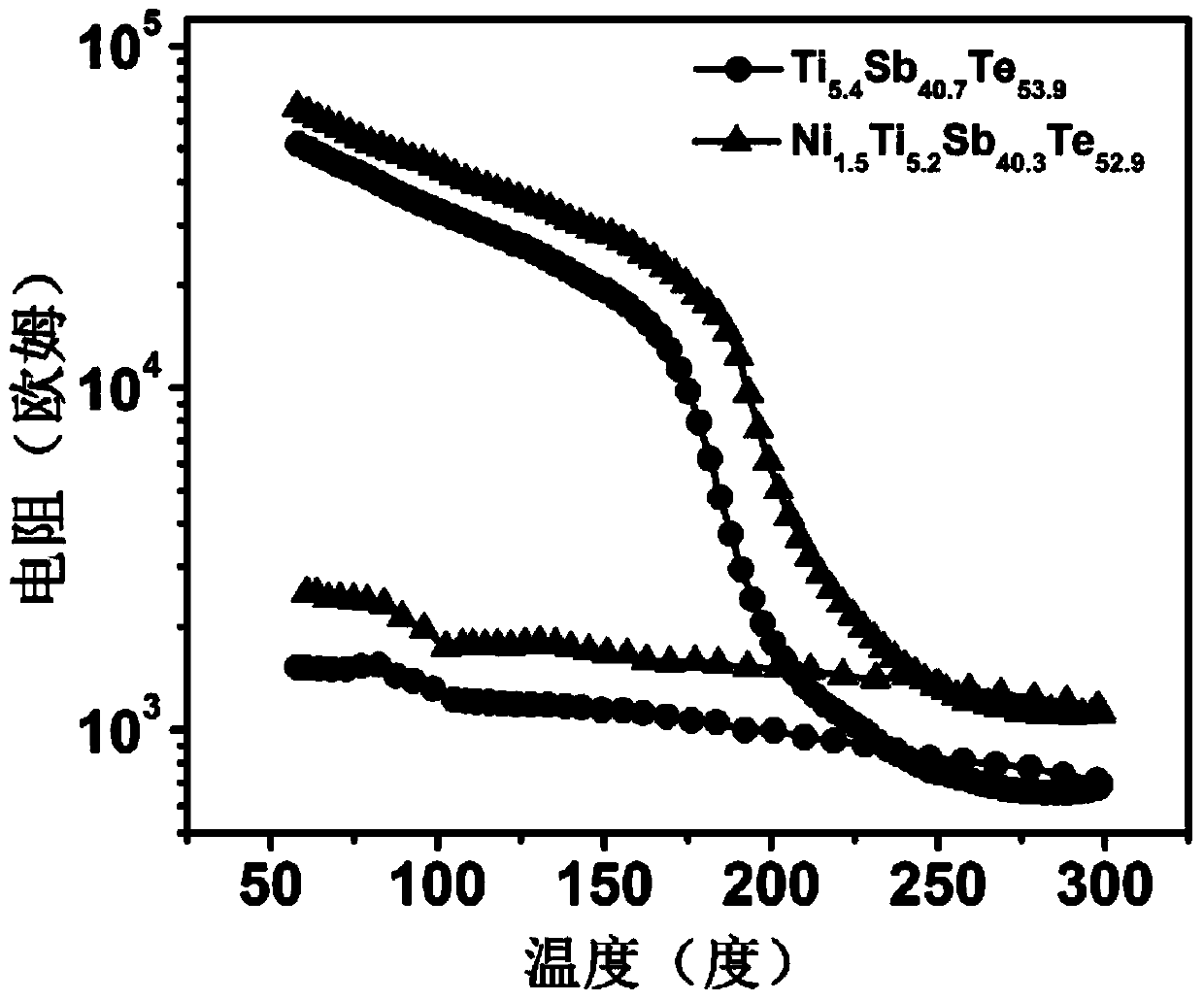
[0048] As an example, the phase change thin film material includes an amorphous state and a crystalline state, and the ratio of the resistivity of the amorphous state to the resistivity of the crystalline state of the phase change thin film material is greater than or equal to 5.
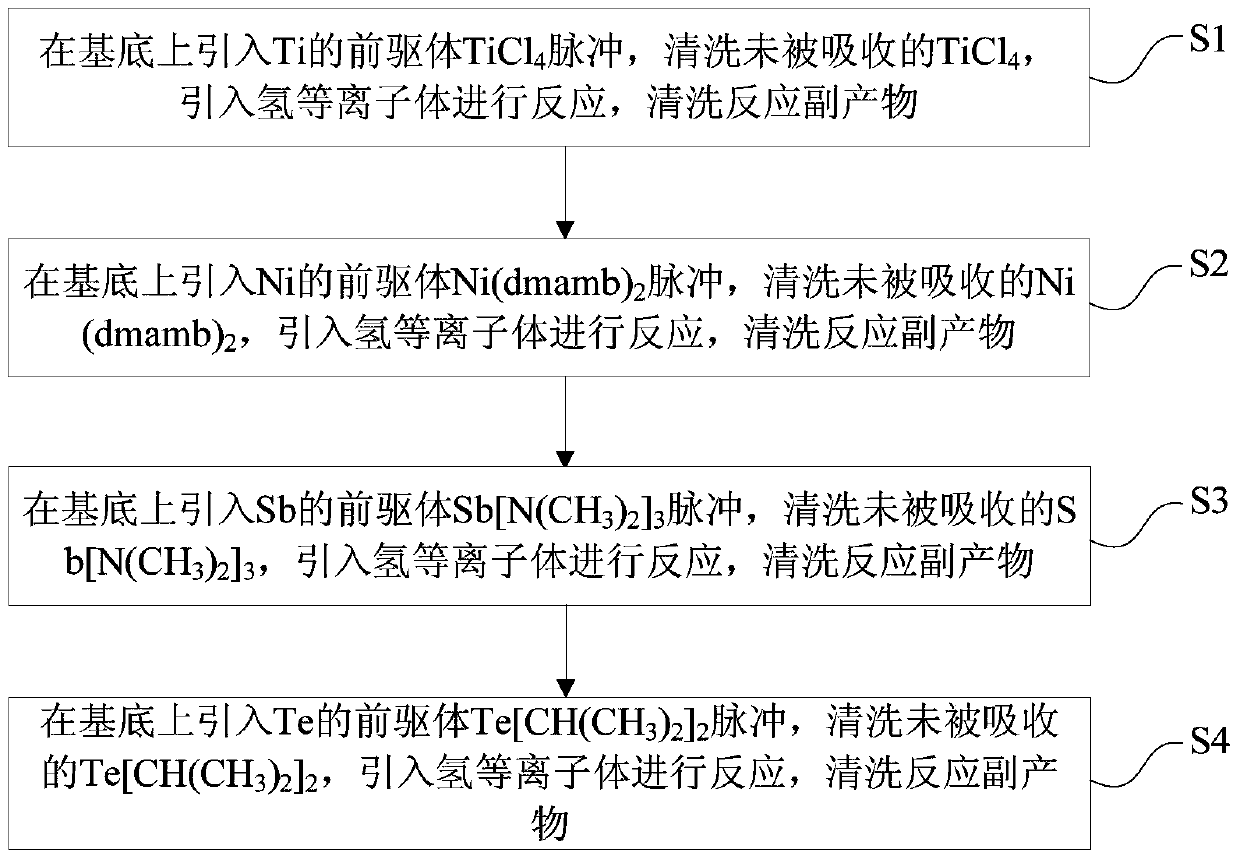
[0049] see figure 1 , the present invention also provides a kind of preparation method of phase-change film material as described above, and described preparation method comprises the following steps:
[0050] S1: Introdu...
Embodiment 2
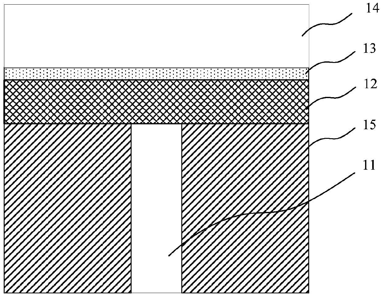
[0078] The present invention also provides a phase-change memory unit, which includes the phase-change thin film material as described in the first embodiment. The phase-change memory unit can be various cell structures of the existing phase-change memory, please refer to image 3 , In one embodiment, the phase change memory unit includes: an insulating dielectric layer 15, a lower electrode 11, a phase change thin film material 12 as described in Embodiment 1, a transition layer 13 and an upper electrode 14; the lower electrode 11 is located in the insulating dielectric layer 15 and runs through the insulating dielectric layer 15; the phase change film material 12 is located on the upper surface of the insulating dielectric layer 15 and is located directly above the lower electrode 11; the The transition layer 13 is located on the upper surface of the phase change film material 12 ; the upper electrode 14 is located on the upper surface of the transition layer 13 .
[0079] ...
PUM
| Property | Measurement | Unit |
|---|---|---|
| thickness | aaaaa | aaaaa |
Abstract
Description
Claims
Application Information


