Method of manufacturing surface cross-scale functional micro-nano structure

A manufacturing method and technology of micro-nano structure, which are applied in the fields of nanostructure manufacturing, specific nanostructure formation, manufacturing tools, etc., can solve the problems of low manufacturing efficiency, complex process, high cost, etc., and achieve high processing efficiency, good application prospects, The effect of low-cost manufacturing

Inactive Publication Date: 2017-05-31
LANZHOU INST OF PHYSICS CHINESE ACADEMY OF SPACE TECH
View PDF8 Cites 12 Cited by
  • Summary
  • Abstract
  • Description
  • Claims
  • Application Information

AI Technical Summary

Problems solved by technology

[0003] However, there have always been major technical difficulties in the preparation of micro-nano structures on the surface of structures. The main reason is that the processing of nano-scale structures requires semiconductor processes such as photolithography and corrosion. The equipment is expensive, the process is complicated, the cost is high, and the production efficiency is very

Method used


Image

  • Method of manufacturing surface cross-scale functional micro-nano structure
  • Method of manufacturing surface cross-scale functional micro-nano structure

Examples


Embodiment 1

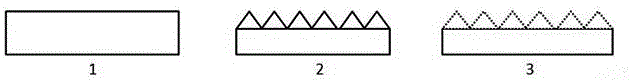
[0017] Such as figure 1 As shown, using a millisecond pulsed laser, using a triangular mask to modulate the beam shape into a triangular spot with a side length of 100 μm at the focal point, using an output power of 200W and a pulse frequency of 1KHz, first along the X-axis direction on the surface of a 5mm titanium alloy ( A high-speed galvanometer is used for scanning on the vertical direction of the bottom edge of the triangular spot, with a scanning distance of 100 μm and a speed of 5 mm / s. After the whole surface scanning process is completed, the titanium alloy workpiece is rotated 90° (Y axis), and then scanned again with the same parameters, and finally the etching process of the conical microstructure (cone) is completed.

[0018] Then use femtosecond pulsed laser, pulse width of 150fs, pulse frequency of 10KHz, spot size of 50μm, first scan and irradiate on the surface of the processed cone along the X-axis direction with a high-speed galvanometer, the scanning dista...

Embodiment 2

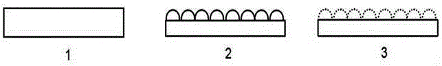
[0020] Such as figure 2 As shown, using a millisecond pulsed laser, using an hourglass-shaped mask to modulate the beam shape into an hourglass-shaped spot with a side length of 300 μm at the focal point, using an output power of 200W and a pulse frequency of 1KHz, the surface of the 5mm aluminum alloy is first along the X-axis The direction is scanned by a high-speed galvanometer with a scanning distance of 300 μm and a speed of 5 mm / s. After the whole surface scanning process is completed, the aluminum alloy workpiece is rotated 90° (Y axis), and then scanned again with the same parameters, and finally the etching process of the semicircular microstructure is completed.

[0021] Then use femtosecond pulsed laser, pulse width of 100fs, pulse frequency of 12KHz, spot size of 100μm, first scan and irradiate the processed semicircular microstructure surface along the X-axis direction with a high-speed galvanometer, and the scanning distance is 100μm , speed 5mm / s. After scann...


PUM


Abstract

The invention discloses a method of manufacturing a surface cross-scale functional micro-nano structure; the method comprises the steps of first, scanning the surface of a base by millisecond pulsed laser to obtain a micro structural graph; scanning the manufactured micro structural graph by femtosecond pulsed laser to obtain manufacture a nano structural graph on the surface of the micro structural graph by induction. By using the method of manufacturing surface micro-nano functional structure combining millisecond pulsed laser etching and femtosecond laser induction, the cross-scale high-performance low-cost manufacture of the micro and nano functional microstructure can be achieved, the manufacturing efficiency is far higher than that of semiconductor process, and the method has a better application prospect.

Description

technical field [0001] The invention relates to the field of material processing, and specifically relates to a method for manufacturing surface cross-scale functional micro-nano structures. Background technique [0002] The preparation of micro-nano structures on the structured surface to achieve functionalization can enable the structured surface to obtain special physical properties that the structural material itself does not have, such as enabling the metal surface with high reflectivity to electromagnetic waves to have high absorption performance and high reflectivity to the solar spectrum. With ultra-high absorption rate, the surface of the ship with high wettability to water has super-wetting characteristics to reduce flow resistance, etc. application. [0003] However, there have always been major technical difficulties in the preparation of micro-nano structures on the surface of structures. The main reason is that the processing of nano-scale structures requires ...

Claims


Application Information

Patent Timeline
IPC IPC(8): B82B3/00B23K26/362B82Y40/00
CPCB82B3/0014B23K26/361B82Y40/00
Inventor 曹生珠何延春张凯锋吴敢陈学康王瑞王虎王兰喜
Owner LANZHOU INST OF PHYSICS CHINESE ACADEMY OF SPACE TECH
Why Eureka
Try Eureka