Method for selectively preparing gold-tin eutectic solder on surface of ceramic substrate
A technology of ceramic substrate and eutectic solder, applied in the field of selective preparation of gold-tin eutectic solder on the surface of ceramic substrate, can solve the problems of reduced heat dissipation efficiency, poor stability of plating solution, influence of heat dissipation effect, etc., and achieves high stability and welding. The effect of good performance and high production efficiency
- Summary
- Abstract
- Description
- Claims
- Application Information
AI Technical Summary
Problems solved by technology
Method used
Image
Examples
Embodiment 1
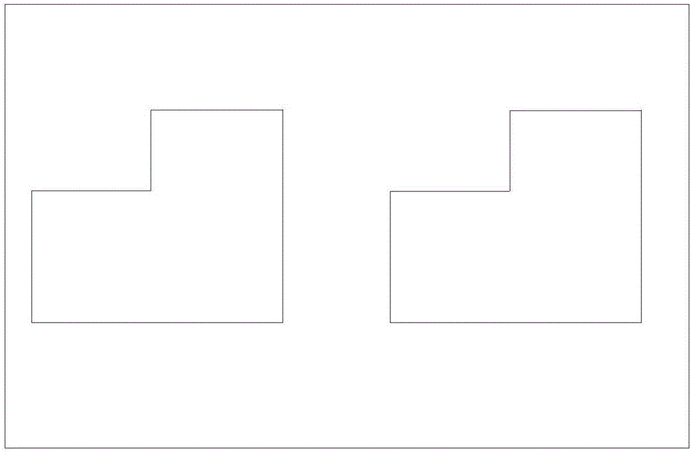
[0025] On an alumina ceramic substrate with a thickness of 0.5 μm, the first conductive layer with a thickness of 20 nm is sputtered, and copper is electroplated as the second conductive layer (50 nm in thickness), and the pattern layer is obtained by photolithography, and then etched copper gets as figure 1 Array graph shown. The gold-tin alloy solder is electroplated on the array pattern, and the gold-tin alloy electroplating solution is a cyanide-free electroplating solution with a pH of 3 to 7, including gold salt, tin salt, brightener, complexing agent and antioxidant, and finally a patterned Au-Sn eutectic solder.
Embodiment 2
[0027] A gold layer (thickness 1nm) is electrochemically plated on a highly thermally conductive aluminum nitride substrate with a thickness of 0.5 μm, and then a patterned gold layer is obtained through a positive resist lithography process and etching technology, and electroplating is realized on the gold layer Gold-tin alloy solder, the electroplating solution is a cyanide-free system, including gold salts, tin salts, brighteners, complexing agents, antioxidants, indium salts, and gallium salts. Finally, the patterned gold-tin eutectic solder is obtained (the enlarged picture of two gold-tin eutectic bumps is shown in figure 2 ).
Embodiment 3
[0029] On the alumina ceramic substrate with a thickness of 5 μm, a gold layer (thickness of
[0030] 100nm), then on the gold layer, obtain a graphic layer through negative resist etching, etch the gold layer with a gold etchant to obtain a patterned gold layer, and realize electroplating gold-tin alloy solder on the gold layer, and the electroplating solution is a cyanide-free system Electroplating solution, including gold salt, tin salt, brightener, complexing agent, antioxidant and indium salt, gallium salt. Finally, a patterned gold-tin eutectic solder is obtained.
PUM
| Property | Measurement | Unit |
|---|---|---|
| Thickness | aaaaa | aaaaa |
| Thickness | aaaaa | aaaaa |
| Thickness | aaaaa | aaaaa |
Abstract
Description
Claims
Application Information

