Method for growing polarity alternate GaN structure on N-polar GaN template

A technology of growing polarity and polarity, which is applied in the direction of electrical components, semiconductor/solid-state device manufacturing, circuits, etc., can solve the problems of high cost of GaN substrates and difficult popularization of GaN structures, and achieve the effect of avoiding damage

Inactive Publication Date: 2017-05-31
UNIV OF SCI & TECH BEIJING
View PDF3 Cites 3 Cited by
  • Summary
  • Abstract
  • Description
  • Claims
  • Application Information

AI Technical Summary

Problems solved by technology

At present, although the use of HVPE and ammonothermal method to prepare GaN bulk materials is becoming more and more mature, the cost of GaN

Method used


Image

  • Method for growing polarity alternate GaN structure on N-polar GaN template
  • Method for growing polarity alternate GaN structure on N-polar GaN template
  • Method for growing polarity alternate GaN structure on N-polar GaN template

Examples


Embodiment 1

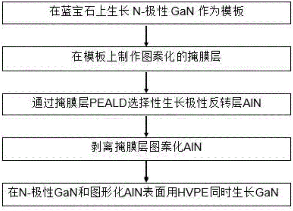
[0049] Methods for growing alternating Ga- and N-polar GaN structures on sapphire substrates:

[0050] Step 1: Clean the sapphire substrate with isopropanol, acetone, methanol, alcohol, and deionized water at room temperature for 5 minutes, and finally wash it with N 2 blow dry.

[0051] Step 2: Put the cleaned sapphire substrate in the N-rich MOCVD reaction chamber, perform nitriding treatment at high temperature, and use triethylgallium TEG and NH 3 As Ga and N sources respectively, grow N-polar GaN with a film thickness of 1.5-2um under the conditions of a temperature of 1100°C, a chamber pressure of 150Torr, and a V / III ratio of 600-3000.

[0052] Step 3: Using N-polar GaN as a template, prepare a patterned photoresist by photolithography: soak the above sample in deionized water for 2 minutes, and then use 80°C standard cleaning solution SC1 (NH 4 0H:H 2 o 2 :H 2 (O=1:1:5) was cleaned for 10 minutes, then cleaned with deionized water and dried with nitrogen, and a la...

Embodiment 2

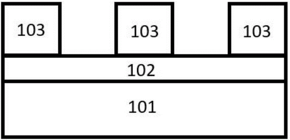
[0057] 1) Refer to figure 2 , the sapphire substrate 101 was ultrasonically cleaned with isopropanol, acetone, methanol, and alcohol at room temperature for 5 minutes, then repeatedly rinsed with deionized water, and washed with N 2 blow dry. The cleaned sapphire substrate 101 is placed in an N-rich MOCVD reaction chamber, and after nitriding treatment at high temperature, it is treated with triethylgallium TEG and NH 3 As Ga and N sources respectively, a 2um N-polar GaN layer 102 is grown under the conditions of a temperature of 1100° C., a chamber pressure of 150 Torr, and a V / III ratio of 3000.

[0058] 2) Refer to image 3 , using N-polar GaN as a template, use a photolithography process to make a patterned photoresist 103: soak the sample in the previous step in deionized water for 2 minutes, and then use 80°C standard cleaning solution SC1 (NH40H: H2O2:H2O=1:1:5) was cleaned for 10 minutes, then cleaned with deionized water and dried with nitrogen, and a layer of pos...


PUM

PropertyMeasurementUnit
Thicknessaaaaaaaaaa
Thicknessaaaaaaaaaa

Abstract

The invention discloses a method for growing polarity alternate GaN structure on N-polar GaN template, belong to the field of semiconductor process and devices. The N-polar GaN grown by MOCVD on sapphire substrate serves as a template, and a patterned photoresist is fabricated on the template as a mask layer by photolithographic process. An AlN selectively grows for polarity inversion on the mask layer with T-ALD method, wherein the T-ALD method can make the process temperature lower than the melting point of the mask layer to ensure that the mask layer is not deformed, and an AlN thin-film with good uniformity and precisely controllable thickness can be prepared. The stripping patterned AlN on the mask layer eliminates the etching step of the traditional patterning process and avoids the damage of the etching to the device structure. Finally, a GaN thick-film grows on the bare N-polar GaN template and the patterned AlN by HVPE method, and a polarity alternate GaN structure with a thickness of 1mm is expected to be obtained to meet the requirements of high-power component for the thick-film polarity alternate GaN.

Description

technical field [0001] The invention relates to the field of semiconductor technology and devices, in particular to a method for growing GaN structures with different polarities on a sapphire substrate. Background technique [0002] Wurtzite-structured GaN has a hexagonal crystal structure, and the positive and negative charges in the C-axis direction are not centrosymmetric, and have an intrinsic polarization effect. In the bonding of N and Ga, the covalent bond electrons are biased towards N, so the spontaneous pole The direction of transformation is N to Ga, and in the +C(0001) direction is Ga to N, showing Ga-polarity, so it shows N-polarity in the -C(000-1) direction, and they have significantly different characteristics , such as chemical activity, doping efficiency, polarization direction, work function, surface morphology and internal electric field, etc. Although hexagonal GaN semiconductors have such different polarities, current GaN-based devices still basically ...

Claims


Application Information

Patent Timeline
IPC IPC(8): H01L21/02
CPCH01L21/02376H01L21/0254
Inventor 刘三姐郑新和彭铭曾侯彩霞王瑾何荧峰李美玲
Owner UNIV OF SCI & TECH BEIJING
Why Eureka
Try Eureka