Power mode Surface Mounted Device (SMD) semiconductor component

A semiconductor and power-type technology, applied in the field of power-type SMD semiconductor components, can solve the problems of withstand power and small current

Pending Publication Date: 2017-05-31
BESTBRIGHT ELECTRONICS
View PDF7 Cites 5 Cited by
  • Summary
  • Abstract
  • Description
  • Claims
  • Application Information

AI Technical Summary

Problems solved by technology

[0005] As can be seen from the above, the withstand power and current of SMD semiconductor components on the market are often relatively small, far lower than traditional plug-in semiconductor components, and in products such as automotive electronics and high-power power supplies, almost The power of kilowatts and the flow capacity of hundreds of amps are far from meeting the needs of actual use, and many products still use plug-in semiconductor components

Method used


Image

  • Power mode Surface Mounted Device (SMD) semiconductor component
  • Power mode Surface Mounted Device (SMD) semiconductor component
  • Power mode Surface Mounted Device (SMD) semiconductor component

Examples


Embodiment 1

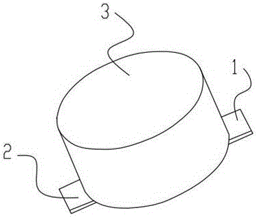
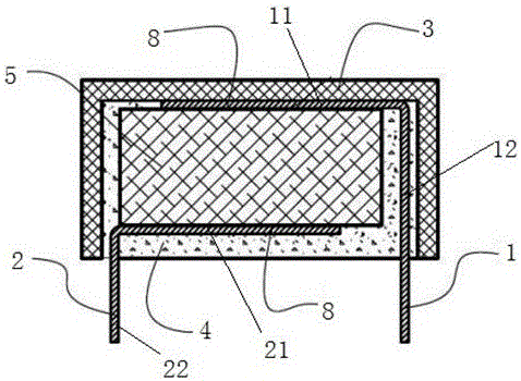
[0033] like figure 2 As shown, the embodiment of the present invention discloses a power chip semiconductor element, including a varistor chip 5, the upper electrode sheet 1 is welded on the upper surface of the varistor chip 5 through a solder sheet 8, and the lower electrode sheet 2. Solder the lower surface of the piezoresistor chip 5 through a solder sheet 8; the outer side of the piezoresistor chip 5 is provided with a container-shaped flame-retardant insulating shell 3, and the gap between the shell and the piezoresistor chip 5 is Filled with encapsulation filler 4, the free ends of the upper electrode sheet 1 and the lower electrode sheet 2 extend out of the casing, serving as two connecting pins of the semiconductor element.

[0034] like figure 2 , 6 As shown, the upper electrode sheet 1 includes a first horizontal welding sheet 11 and a first connecting sheet 12 . The first horizontal soldering piece 11 is welded on the upper surface of the combination chip, the...

Embodiment 2

[0039] This embodiment is different from the first embodiment in that the specific forms of the upper electrode sheet 1 and the lower electrode sheet 2 are different. The first embodiment is a direct plug-in pin component, and the second embodiment is a patch pin component. Specifically, such as image 3 As shown, the upper electrode sheet 1 includes a first horizontal welding sheet 11 and a first connecting sheet 12, the first horizontal welding sheet 11 is welded on the upper surface of the combined chip, and the first connecting sheet 12 includes a first connecting sheet 12 A vertical connection part 121 and a first horizontal connection part 122, the upper end of the first vertical connection part 121 is fixedly connected with the first horizontal welding piece 11, and the lower end of the first vertical connection part 121 is located at the Outside the housing, it is fixedly connected with the first horizontal connection portion 122, and the first horizontal connection po...

Embodiment 3

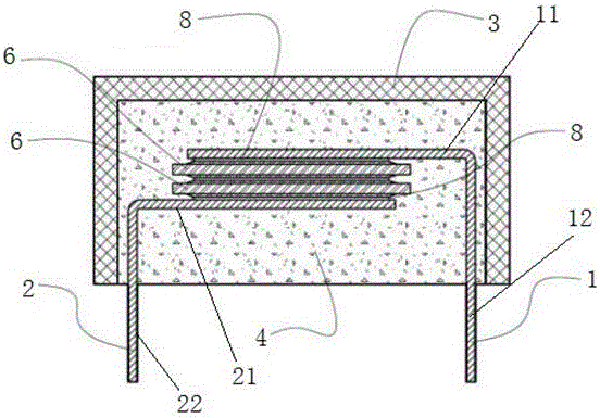
[0041] like Figure 4 As shown, the embodiment of the present invention discloses a power chip semiconductor element, including a combination chip, and the combination chip includes two TVS chips 6 stacked together on top and bottom. The upper and lower surfaces of the TVS diode chip 6 are provided with a conductive nickel layer, between the TVS diode chip 6 and the TVS diode chip 6 and between the upper electrode sheet 1 and the lower electrode sheet 2 and the TVS diode chip 6 are welded through solder sheet 8. The outer side of the combined chip is provided with a container-shaped flame-retardant insulating shell 3, and an encapsulation filler 4 is filled between the shell and the combined chip, and the free ends of the upper electrode sheet 1 and the lower electrode sheet 2 extend to the Outside the housing, as the two connecting pins of the semiconductor element.

[0042] like Figure 4 , 6 As shown, the upper electrode sheet 1 includes a first horizontal welding sheet...


PUM


Abstract

The invention discloses power mode Surface Mounted Device (SMD) semiconductor components, and relates to the technical field of electronic components. The semiconductor components comprise combination chips, upper electrode sheets are welded on the upper surfaces of the combination chips, lower electrode sheets are welded on the lower surfaces; a container-shape flame retardant insulation shell is arranged on the outer side of the combination chips, the space between the shell and the combination chips is filled with package fillers, the free ends of the upper electrode sheet and the lower electrode sheet extend to the shell outside, to act as the two connection pins of the semiconductor components. According to the semiconductor components, semiconductor chips which are the same with the traditional plug-in type semiconductor components can be packaged, and can keep at the same level with the plug-in components in power and other electrical property indexes; the electrode sheets and semiconductor chip are loaded into the shell after the welding is completed, and package filler are filled, the filled package filler has flame retardant characteristics, and the shell is also of flame retardant material, the whole semiconductor chip is packaged by the flame retardant material, and fire can be effectively blocked.

Description

technical field [0001] The invention relates to the technical field of electronic components, in particular to a power chip semiconductor component. Background technique [0002] The semiconductor protection components mainly used in the market now include transient suppressor diode TVS of silicon or silicon carbide chip, silicon avalanche diode ABD, thyristor suppressor TSS or varistor MOV of metal oxide chip. [0003] The above-mentioned transient suppression diode TVS, silicon avalanche diode ABD, and thyristor suppressor TSS are generally packaged in SOD-123, DO-214AA, DO-214AB, DO-214AC, etc., and the current they can withstand ranges from several amperes to several Hundreds of amps range, and can withstand power from 200W to a maximum of 6.5kW. The traditional in-line components can withstand a current of several thousand amperes and a power of up to 30kW. [0004] Chip varistors with metal oxide material chips on the market now mainly include multilayer ceramic stru...

Claims


Application Information

Patent Timeline
Patent Type & Authority Applications(China)
IPC IPC(8): H01L23/488H01L23/06H01L23/18
CPCH01L23/06H01L23/18H01L23/488
Inventor 张晗周云福黄亚发
Owner BESTBRIGHT ELECTRONICS
Why Eureka
Try Eureka