FPC board light source packaging structure and production method thereof
A packaging structure and light source technology, applied in the direction of electrical components, electric solid devices, circuits, etc., can solve the problems of inflexibility or small bending range, high calorific value, and inability to increase power, and achieve high price and low calorific value. Effect
- Summary
- Abstract
- Description
- Claims
- Application Information
AI Technical Summary
Problems solved by technology
Method used
Image
Examples
Embodiment 1
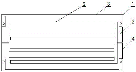
[0033] Such as figure 1 As shown, the FPC board light source packaging structure described in the embodiment of the present invention is composed of an FPC packaging board 1, the outer surface of the FPC packaging board 1 has a fluorescent powder adhesive layer 2, and the inside of the fluorescent powder adhesive layer 2 is flip-chip. A chip encapsulation layer 5 is encapsulated by means of a method, and the two ends of the chip encapsulation layer 5 are provided with positive and negative electrode areas of the chip;
[0034] Further, the left and right sides of the FPC packaging plate 1 are all short sides of the same length and serve as the arrangement side 4, and at the same time, the upper and lower sides of the FPC package plate 1 are all long sides of the same length and are used as the bending side 3. The positive and negative poles of the chip packaging layer 5 are respectively located in the packaging area close to the bending edge 3, and since the positive and negat...
Embodiment 2
[0036] Such as figure 1 As shown, the FPC board light source packaging structure described in the embodiment of the present invention is composed of an FPC packaging board 1, the outer surface of the FPC packaging board 1 has a fluorescent powder adhesive layer 2, and the inside of the fluorescent powder adhesive layer 2 is flip-chip. A chip encapsulation layer 5 is encapsulated by means of a method, and the two ends of the chip encapsulation layer 5 are provided with positive and negative electrode areas of the chip;
[0037] Further, the left and right sides of the FPC packaging plate 1 are short sides of the same length and used as bending edges, and at the same time, the upper and lower sides of the FPC packaging plate 1 are long sides of the same length and used as the arrangement side, The positive and negative poles of the chip packaging layer 5 are respectively located in the packaging area close to the bending, and since the positive and negative poles of the chip are...
Embodiment 3
[0039] Such as figure 1 As shown, a production method of an FPC board light source packaging structure consists of the following steps,
[0040] ⑴First carry out the crystal-bonding operation, put the FPC board into the fixture, adjust the program of the crystal-bonding machine, and start the crystal-bonding;
[0041] ⑵ Reflow soldering operation, adjust the temperature of each temperature zone of the reflow soldering, put the solid crystal product together with the fixture into the reflow soldering for reflow soldering;
[0042] (3) Test the reflowed products;
[0043] ⑷The dam is required according to the size of the light-emitting surface;
[0044] ⑸ Prepare phosphor glue according to the requirements of each optical parameter, stir and defoam, and perform glue filling operation;
[0045] ⑹ Put the glued product into the oven for baking;
[0046] ⑺ After cooling at room temperature, remove the fixture cover, and pack the product into storage after optical and electrical...
PUM
 Abstract
Description
Claims
Application Information
