Optical interface device of optical demultiplexer/multiplexer for high-speed optical module
An optical module and optical demultiplexing technology, which is applied in the field of optical communication and can solve the problems of large installation and operation difficulty of optical transceiver components and demultiplexers, fiber damage or breakage, and unqualified optical modules.
- Summary
- Abstract
- Description
- Claims
- Application Information
AI Technical Summary
Problems solved by technology
Method used
Image
Examples
Embodiment approach 1
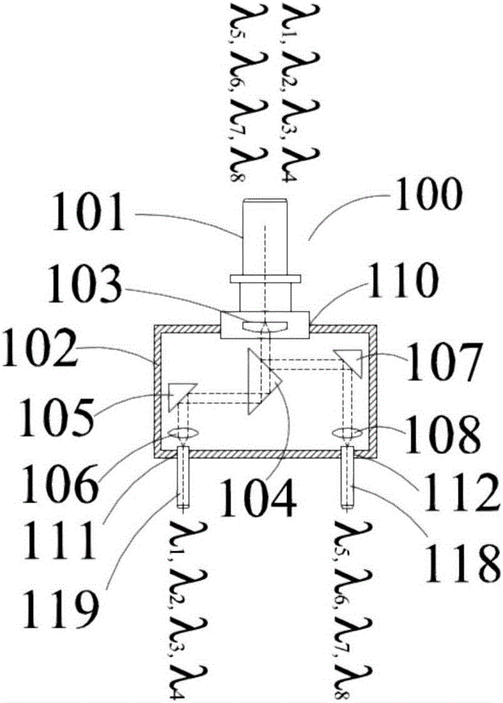
[0036] An optical interface device for an optical splitter and multiplexer for high-speed optical modules provided by the present invention, the internal structure and function block diagram of the first embodiment is as follows figure 2 As shown, it includes: a packaging case 102, an external optical interface unit 100, two internal optical interface units 118 and 119, and an optical splitting or combining optical unit. Wherein: the packaging case 102 includes an installation space, and provides a coupling hole 110 for the external interface, and two coupling holes 111 and 112 for the internal interface. Wherein, the installation and assembly space is used for installing and fixing the packaged optical splitting or multiplexing optical unit. The external interface coupling hole 110 is used for installing the external optical interface unit 100 , and the size of the external interface coupling hole 110 should allow the external optical interface unit 100 to be partially inser...
Embodiment approach 2
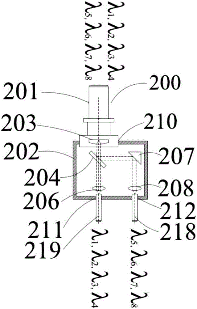
[0045] The functional block diagram of the internal structure of Embodiment 2 of the present invention is as follows image 3 As shown, it includes a packaging case 202, an external optical interface unit 200, two internal optical interface units 218 and 219, and an optical splitting or combining optical unit. The functions / structures of the external optical interface unit 200 and the internal optical interface units 218 and 219 are the same as those described in the first embodiment. The packaging case 202 includes an installation and assembly space, and provides a coupling hole 210 for the external interface, and two coupling holes 211 and 212 for the internal interface. The above coupling holes are also consistent with the functions / structures described in the corresponding components in Embodiment 1 . The difference between Embodiment 2 and Embodiment 1 mainly lies in the structure of the optical unit for optical wave splitting or multiplexing. In Embodiment 2, a light wa...
Embodiment approach 3
[0049] Embodiment 3 is a symmetrical structure of Embodiment 2, and its function and implementation are consistent with 2, such as Figure 4 shown.
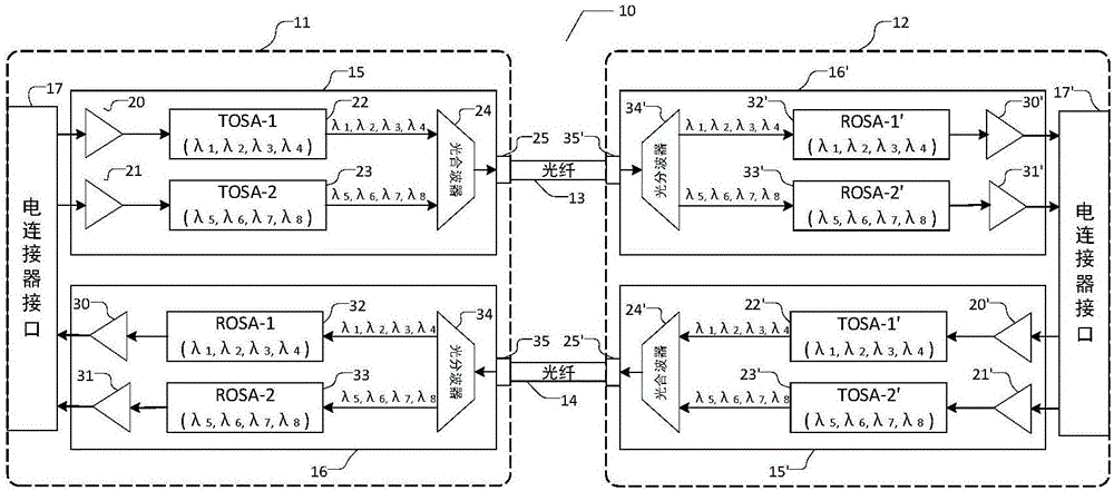
[0050] λ described in the present invention 1 ,λ 2 ,λ 3 ,λ 4 ,λ 5 ,λ 6 ,λ 7 ,λ 8 The eight wavelengths are LAN-WDM wavelengths defined by the IEEE802.3bj standard.
[0051] The optical port device of the optical demultiplexer and multiplexer described in the present invention can be installed in CFP series and QSFP-DD high-speed optical module packaging structures.
[0052] In the present invention, the positions of the external and internal interfaces can be adjusted according to the definition of the size of the high-speed optical module, but the overall frame will not change fundamentally. At the same time, the turning edges and corners added in the optical path can adjust the optical path at a small angle, compensating for the device processing and The optical path mismatch caused by assembly greatly reduces the requ...
PUM
 Abstract
Description
Claims
Application Information


