Metallic oxide semiconductor field effect transistor and manufacturing method thereof
A field-effect transistor, oxide semiconductor technology, applied in semiconductor/solid-state device manufacturing, semiconductor devices, electrical components, etc., can solve problems such as limiting breakdown field strength, gate-to-drain breakdown, and uneven electric field distribution of devices , to achieve the effect of weakening aggregation and increasing reverse breakdown voltage
- Summary
- Abstract
- Description
- Claims
- Application Information
AI Technical Summary
Problems solved by technology
Method used
Image

Examples
example 1
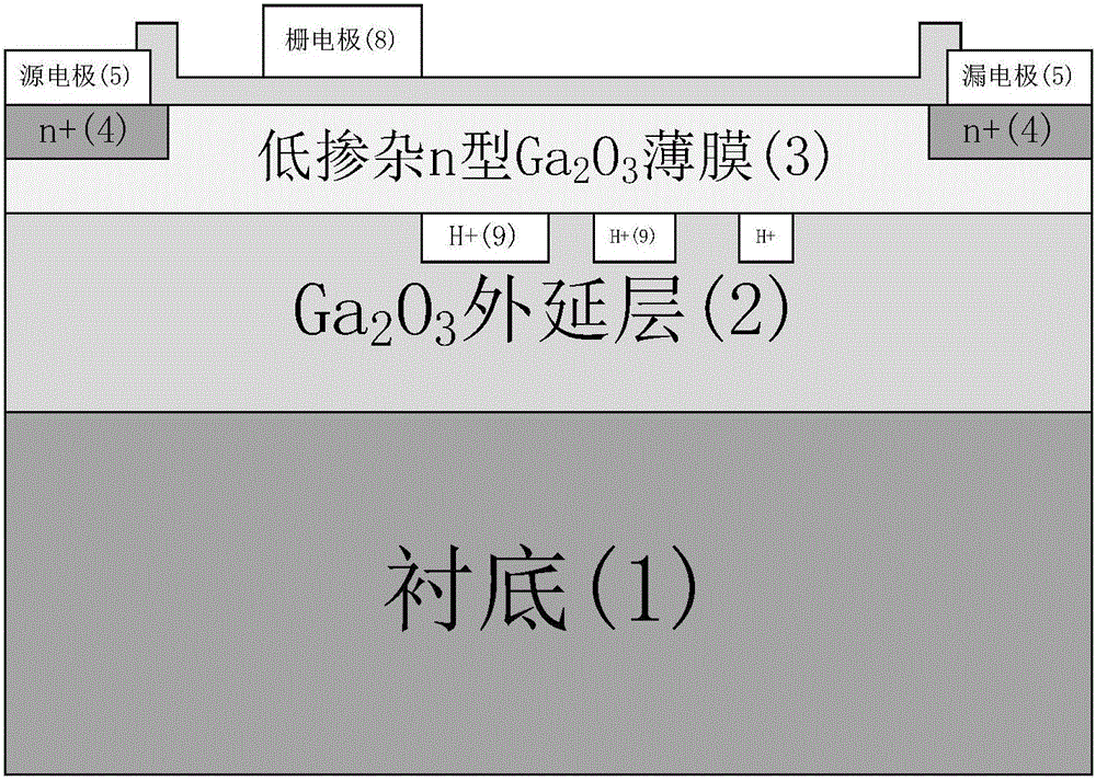
[0039] Example 1, making the substrate as Ga 2 o 3 , Si ions are implanted, and the insulating gate dielectric is Al 2 o 3 Metal Oxide Semiconductor Field Effect Transistors.
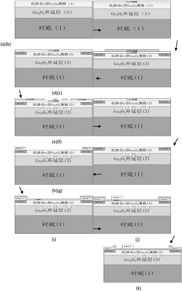
[0040] Step 1: Wash the sample as figure 2 (a) shown.
[0041] 1a) First, the epitaxially grown Ga on the substrate 2 o 3 The samples were cleaned organically, washed with flowing deionized water, and put into HF:H 2 Corrosion in the solution of O=1:1 for 60s;
[0042] 1b) The corroded sample was washed with flowing deionized water, and dried with high-purity nitrogen.
[0043] Step 2: Deposit SiO 2 mask, such as figure 2 (b) shown.
[0044] Put the cleaned sample into the PECVD equipment, set the reaction chamber pressure to 2Pa, the RF power to 40W, and simultaneously feed SiH with a flow rate of 40sccm 4 and a flow rate of 10 sccm N 2 O, in n-type Ga 2 o 3 SiO with a thickness of 50 nm was deposited on the film 2 mask.
[0045] Step 3: Make the ion implantation area, such as figu...
example 2
[0067] Example 2, the production substrate is sapphire, implanted with Sn ions, and the insulating gate dielectric is HfO 2 Metal Oxide Semiconductor Field Effect Transistors.
[0068] Step 1: Wash the sample, such as figure 2 (a) shown.
[0069] This step is the same as Step 1 of Example 1.
[0070] Step 2: Deposit SiO 2 mask, such as figure 2 (b) shown.
[0071] This step is the same as Step 2 of Example 1.
[0072] Step 3: Make the ion implantation area, such as figure 2 (c) shown.
[0073] 3.1) To complete SiO 2 The sample deposited by the mask is subjected to photolithography to form an ion implantation area;
[0074] 3.2) Put the photolithographic sample into the ion implantation reaction chamber to perform Sn ion implantation twice, the first implantation energy is 60keV, and the implantation dose is 3.2×10 14 cm -3 ; The second implantation energy is 30keV, and the implantation dose is 9.3×10 13 cm -3 ;
[0075] Step 4: Degelling and annealing activati...
example 3
[0091] Example 3, making the substrate as MgAl 2 o 4 , Ge ions are implanted, and the insulating gate dielectric is Si 3 N 4 Metal Oxide Semiconductor Field Effect Transistors.
[0092] Step A: Wash the sample as figure 2 (a) shown.
[0093] This step is the same as Step 1 of Example 1.
[0094] Step B: Deposit SiO 2 mask, such as figure 2 (b) shown.
[0095] This step is the same as Step 2 of Example 1.
[0096] Step C: Make the ion implantation area: that is, complete the SiO 2 Mask-deposited samples were subjected to photolithography to form ion implantation regions; then the photolithographic samples were placed in the ion implantation reaction chamber for two Ge ion implantations, the first implantation energy was 60keV, and the implantation dose was 3.2×10 14 cm -3 ; The second implantation energy is 30keV, and the implantation dose is 9.3×10 13 cm -3 ;like figure 2 (c) shown.
[0097] Step D: Degelling annealing activation, such as figure 2 (d) shown...
PUM
| Property | Measurement | Unit |
|---|---|---|
| Depth | aaaaa | aaaaa |
| Thickness | aaaaa | aaaaa |
| Thickness | aaaaa | aaaaa |
Abstract
Description
Claims
Application Information