Method of forming a fin field effect transistor

A fin field effect and transistor technology, which is applied in the fields of semiconductor devices, semiconductor/solid-state device manufacturing, electrical components, etc., can solve the problem that the performance of transistors needs to be improved, and achieve the effect of improving punch-through, accurate position, and increasing hot carriers. The effect of the injection effect

Active Publication Date: 2019-11-29
SEMICON MFG INT (SHANGHAI) CORP +1
View PDF4 Cites 0 Cited by
  • Summary
  • Abstract
  • Description
  • Claims
  • Application Information

AI Technical Summary

Problems solved by technology

[0004] The performance of the existing fin field effect transistors still needs to be improved

Method used


Image

  • Method of forming a fin field effect transistor
  • Method of forming a fin field effect transistor
  • Method of forming a fin field effect transistor

Examples


Embodiment Construction

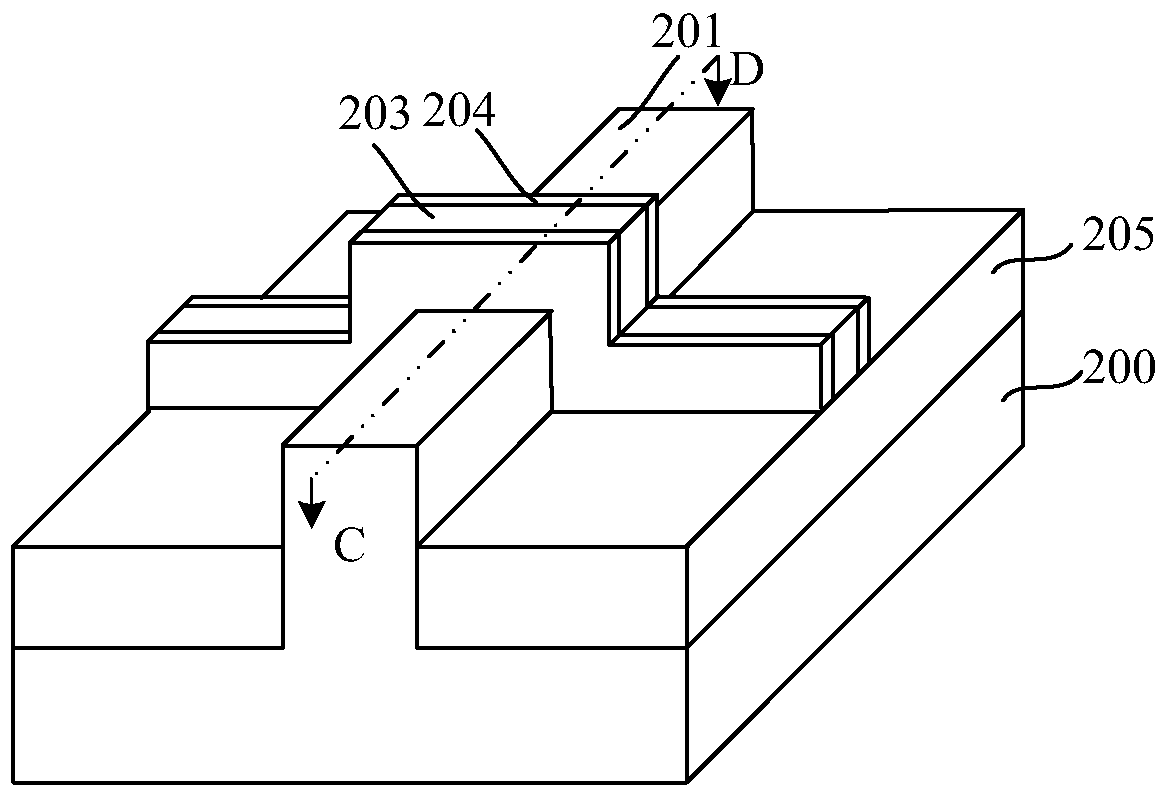
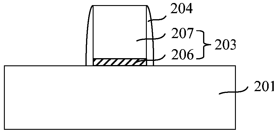
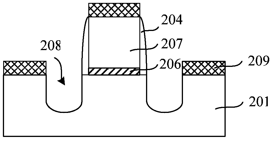
[0042] The performance of the fin field effect transistor formed by the prior art still needs to be improved, for example, the fin field effect transistor formed by the prior art will still be affected by the hot carrier injection effect.

[0043] The study found that the prior art uses ion implantation to form shallowly doped source and drain regions. Due to the three-dimensional structure of the fin, it is affected by the shadow effect, and some positions in the fin may not be implanted with impurity ions or the implanted impurity ions may be affected. Rarely, the concentration distribution of the impurity ions forming the shallowly doped source and drain regions in the fin will be uneven. In addition, the same problem also exists when forming the anti-puncture doping region. The concentration of impurity ions in the anti-puncture doping region is not uniform, so that the anti-puncture performance of the FinFET is also affected.

[0044] An embodiment of the present inventio...


PUM


Abstract

The invention provides a formation method of a fin-type field effect transistor. The method comprises: a semiconductor substrate is provided and a protruding fin part is formed on the semiconductor substrate; a gate structure stretching across and covering the side wall of the partial fin part and the top surface is formed; the fin part at the two sides of the gate structure is etched to form grooves; sacrificial layers doped with impurity ions are formed on the side walls and the bottom surface of the grooves; annealing is carried out on the sacrificial layers doped with impurity ions and thus the impurity ions in the sacrificial layers are diffused in the fin part in contact with the grooves to form a doping region; and then the sacrificial layers are removed. With the method, the impurity ions in the doping region can be distributed uniformly and the position of the doping region becomes accurate, so that an effect of preventing hot carrier injection or preventing punchthrough between source and drain regions can be improved.

Description

technical field [0001] The invention relates to the field of semiconductor manufacturing, in particular to a method for forming a fin field effect transistor. Background technique [0002] In the present invention, with the continuous development of semiconductor process technology, the process node is gradually reduced, and the gate-last process is widely used to obtain an ideal threshold voltage and improve device performance. However, when the feature size (CD, Critical Dimension) of the device is further reduced, even if the gate-last process is adopted, the structure of the conventional MOS field effect transistor can no longer meet the requirements for device performance, and the fin field effect transistor (Fin FET) as Substitution of conventional devices has received extensive attention. [0003] A method for forming a Fin Field Effect Transistor in the prior art includes: providing a semiconductor substrate on which protruding fins are formed, and the fins are gene...

Claims


Application Information

Patent Timeline
Patent Type & Authority Patents(China)
IPC IPC(8): H01L21/336H01L29/78
CPCH01L29/66803H01L29/785
Inventor 禹国宾
Owner SEMICON MFG INT (SHANGHAI) CORP
Why Eureka
Try Eureka