SiC dual-groove metal-oxide-semiconductor field-effect transistor (MOSFET) device integrated with Schottky diode and fabrication method of SiC dual-groove MOSFET device

A Schottky diode and double-groove technology, which is applied in semiconductor/solid-state device manufacturing, electric solid-state devices, semiconductor devices, etc., can solve problems such as poor reliability of gate dielectrics, concentrated electric field, and easy breakdown of gate dielectrics. Increase reliability and prevent punch-through

Active Publication Date: 2017-06-20
BEIJING CENTURY GOLDRAY SEMICON CO LTD
View PDF4 Cites 58 Cited by
  • Summary
  • Abstract
  • Description
  • Claims
  • Application Information

AI Technical Summary

Problems solved by technology

However, UMOSFET has the problem that the electric field at the bottom of the trench is concentrated, so that the reliability of the gate dielectric is poor.
like figure 1 As shown, it is a schematic diagram of a conventional n-channel UMOSFET cell structure. In the off state, the high voltage applied to the drain will act on the drift layer, and the point A at the bottom of the trench will be the most concentrated electric field place, and the electric field strength in the dielectric is 2-3 times that of SiC, causing the gate dielectric at the bottom of the trench to be easily broken down, and the reliability is poor

Method used


Image

  • SiC dual-groove metal-oxide-semiconductor field-effect transistor (MOSFET) device integrated with Schottky diode and fabrication method of SiC dual-groove MOSFET device
  • SiC dual-groove metal-oxide-semiconductor field-effect transistor (MOSFET) device integrated with Schottky diode and fabrication method of SiC dual-groove MOSFET device
  • SiC dual-groove metal-oxide-semiconductor field-effect transistor (MOSFET) device integrated with Schottky diode and fabrication method of SiC dual-groove MOSFET device

Examples


Embodiment Construction

[0045] The present invention will now be described more fully with reference to the accompanying drawings, in which exemplary embodiments of the invention are shown. This invention may, however, be embodied in many different forms and should not be construed as limited to the exemplary embodiments set forth herein. Rather, these embodiments are provided so that this disclosure will be thorough and complete, and will fully convey the scope of the invention to those skilled in the art.

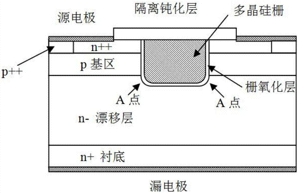
[0046] like figure 2 As shown, the present invention provides a SiC double-groove MOSFET device with an integrated Schottky diode. The original cell structure of the active region of the SiC double-groove MOSFET device is sequentially drain and n+ substrate from bottom to top , buffer layer, n-drift layer, p base region and n++ layer; two grooves are arranged in the original cell structure, which are respectively arranged in the gate groove in the center of the original cell structure and the ...


PUM


Abstract

The invention discloses a SiC dual-groove metal-oxide-semiconductor field-effect transistor (MOSFET) device integrated with a Schottky diode. Two grooves are formed in an original cell structure of an active region in the SiC dual-groove MOSFET device and are respectively a gate groove and a source groove, the gate groove is formed in the center of the original cell structure, the source groove is formed in the periphery of the gate groove, doping with a conductive type opposite to that of a drift region is performed in the peripheries of the bottoms of the gate groove and the source groove, Schottky contact is arranged at a central region of the bottom of the source groove, and the Schottky diode electrically communicating with a source is formed, ohmic contact is formed between the periphery of the bottom of the source groove and a doping region with the conductive type opposite to that of the drift region, and the depths of the two grooves are larger than that of a p base region. With the adoption of a source and gate dual-groove structure, the doping with the conductive type opposite to that of the drift region is performed on the peripheries of the bottoms of the gate groove and the bottom of the source groove, thus, the shielding of an MOS gate is achieved, and the gate reliability is improved; and meanwhile, an electric field of the base region can be shielded, and the base region is prevented from being penetrated; and moreover, an MPS Schottky diode having high surge capability is integrated.

Description

technical field [0001] The invention belongs to the field of semiconductors, and in particular relates to a SiC double-groove MOSFET device integrating Schottky diodes and a preparation method thereof. Background technique [0002] SiC U-type trench MOSFET (UMOSFET) has many advantages, such as the p-base region can be formed by epitaxial growth, which eliminates the influence of defects when ion implantation forms the p-base region, and has better MOS gate quality and channel mobility , and easier to control the channel length. In addition, the original cell structure (basic unit of the active region of the device) of the trench MOSFET can be made smaller and the current density is higher, especially for the expensive price of SiC materials, which can significantly reduce the cost of the chip. However, UMOSFET has the problem that the electric field at the bottom of the trench is concentrated, so that the reliability of the gate dielectric is poor. like figure 1 As shown...

Claims


Application Information

Patent Timeline
Patent Type & Authority Applications(China)
IPC IPC(8): H01L29/872H01L27/06H01L29/78H01L21/77
CPCH01L21/77H01L27/06H01L29/78H01L29/8725
Inventor 倪炜江徐妙玲卢小东
Owner BEIJING CENTURY GOLDRAY SEMICON CO LTD
Why Eureka
Try Eureka