
Vacuum-semiconductor hybrid photoelectric detector

A photodetector and semiconductor technology, applied in the field of photodetectors, can solve the problems such as the inability to meet the detection needs of a large area, the failure to use an electronic optical system to reduce the magnification, and the inability to apply the detector type, etc., so as to improve the effective detection area, The effect of high versatility of device structure and low cost

Inactive Publication Date: 2017-06-20
NO 55 INST CHINA ELECTRONIC SCI & TECHNOLOGYGROUP CO LTD
View PDF6 Cites 3 Cited by
  • Summary
  • Abstract
  • Description
  • Claims
  • Application Information

AI Technical Summary

Problems solved by technology

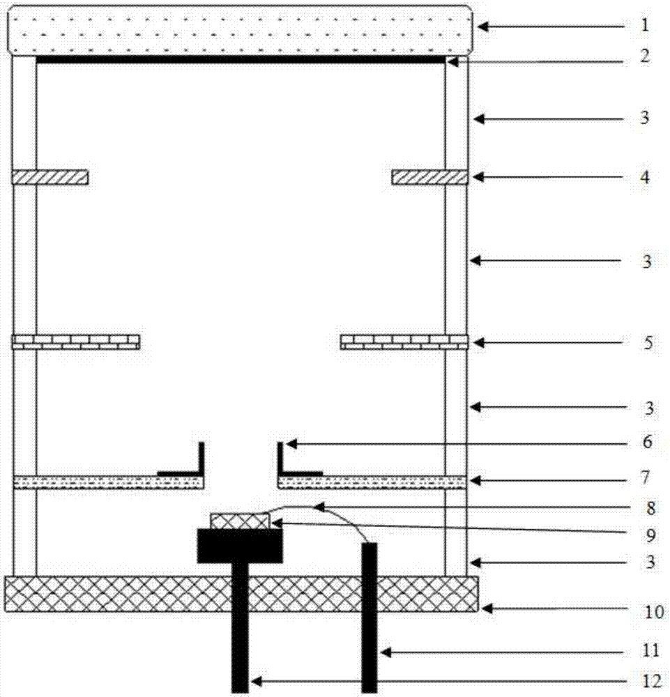
[0004] At present, hybrid devices at home and abroad generally have problems such as small detection area and non-universal device structure. Most of the hybrid devices do not use electron optical systems or the electron optical systems used have low reduction magnifications, which cannot meet the needs of large-scale applications. Detection requirements, and the structures of these devices are customized, which cannot be applied to the needs of different photocathodes and different types of semiconductor detectors

Method used


Image

  • Vacuum-semiconductor hybrid photoelectric detector

Examples


Embodiment Construction

[0012] The technical solutions of the present invention will be further described below in conjunction with the accompanying drawings and embodiments.

[0013] like figure 1 Shown is a vacuum-semiconductor hybrid photodetector according to the present invention, which includes a photocathode 2 and a semiconductor detector 9 as an anode, and also includes a focusing device and a signal output device. The photoelectrons generated by the photocathode 2 are focused and accelerated by the focusing device and then bombarded on the semiconductor detector 9 to generate a gain of thousands of times. The generated electron-hole pairs are collected by the semiconductor detector 9, and then the signal output is realized through the signal output device. The size of the semiconductor detector 9 as the anode is smaller than that of the photocathode 2, which can well increase the effective detection area of ​​the photodetector, increase the bombardment gain, and double the signal strength. ...


PUM


Abstract

The invention discloses a vacuum-semiconductor hybrid photoelectric detector. The vacuum-semiconductor hybrid photoelectric detector includes an input light window, a photoelectric cathode, a ceramic ring, a focusing device, a semiconductor detector, an anode pedestal and a signal output apparatus, wherein the photoelectric cathode is fixed on the input light window; the semiconductor detector is fixed on the signal output apparatus; the signal output apparatus is fixed on the anode pedestal; the focusing device is arranged between the photoelectric cathode and the semiconductor detector; and distance control and insulation can be realized through the ceramic ring between the input light window and the focusing device, and between the focusing device and the anode pedestal. The vacuum-semiconductor hybrid photoelectric detector organically integrates a vacuum device with a semiconductor device, and has the advantages of being large in the detection photosensitive area, being flexible in response to spectrum, being high in the response speed, being large in the dynamic range, being high in gain, being low in dark count, being simple in processing, being convenient in assembling, being low in cost, and being high in reliability.

Description

technical field [0001] The invention relates to a photodetector, in particular to a vacuum-semiconductor hybrid photodetector. Background technique [0002] Photoelectric detection has broad application prospects and great strategic value, and has become a technical field vigorously developed by various countries. Among many photodetectors, the hybrid photodetector is a new type of photodetector developed in the 1990s, which combines the advantages of vacuum photoelectric devices and semiconductor photoelectric devices, and makes up for the shortcomings and deficiencies of both. It is used in high-energy physics, medical instruments, biological detection, quantum communication, astronomical observation and laser ranging and other fields. [0003] The whole tube of the hybrid photodetector adopts the metal-ceramic structure of the vacuum photoelectric device, the cathode adopts the photocathode of the vacuum device, and the anode is a semiconductor detector. During operatio...

Claims


Application Information

Patent Timeline
Patent Type & Authority Applications(China)
IPC IPC(8): H01L31/09H01L31/0232
CPCH01L31/09H01L31/02327
Inventor 徐鹏霄赵文锦王霄唐家业周剑明唐光华戴丽英姚勇汪述猛
Owner NO 55 INST CHINA ELECTRONIC SCI & TECHNOLOGYGROUP CO LTD
Learn More