Graphene photoluminescent substrate and preparation method and application thereof

A technology of photoluminescence and photoluminescent materials, which is applied in the field of graphene photoluminescent substrates and its preparation, can solve problems such as the decline of luminescent performance of photoluminescent materials, the overall design complexity of light-emitting devices, and the overheating of photoluminescent materials.

Pending Publication Date: 2017-07-04
滁州市量子光电有限公司
View PDF5 Cites 2 Cited by
  • Summary
  • Abstract
  • Description
  • Claims
  • Application Information

AI Technical Summary

Problems solved by technology

[0003] In the prior art, the photoluminescent material is usually directly coated on the surface of the LED chip, but this technology is only suitable for photoluminescent materials that are not highly sensitive to temperature, because the surface temperature of the LED chip is relatively high when it is working. , for photoluminescent materials with high temperature sensitivity, such as inorganic semiconductor materials with high color purity, there will be a problem that the luminescence performance of photoluminescent materials will decrease due to high operating temperature
Although there is also a remote excitation technology that places the photoluminescent material at a certain distance from the LED chip to solve the problem of overheating of the photoluminescent material, this will also bring about a significant increase in cost and complex overall design of the light-emitting device. A series of problems, which are greatly limited in practical application

Method used


Image

  • Graphene photoluminescent substrate and preparation method and application thereof

Examples


preparation example Construction

[0042] The present invention provides the preparation method of graphene photoluminescence substrate described in above-mentioned technical scheme, comprises the following steps:

[0043] The photoluminescent material is mixed with the dispersant, and the obtained photoluminescent material dispersion is coated inside the interlayer formed by the graphene layer to form a photoluminescent material layer to obtain a graphene photoluminescent substrate.

[0044] In the present invention, the preparation method of the graphene photoluminescent substrate comprises the following steps: mixing the photoluminescent material with a dispersant, and coating the obtained photoluminescent material dispersion inside the interlayer formed by the graphene layer , forming a photoluminescent material layer to obtain a graphene photoluminescent substrate. In the present invention, there is no special limitation on the type of the dispersant, and a compound known to those skilled in the art that c...

Embodiment 1

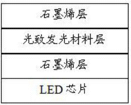
[0067] The preparation structure is successively graphene photoluminescence substrate of graphene layer, photoluminescence material layer, graphene layer, comprises the following steps:

[0068]Polyphenylene vinylene was mixed with chlorobenzene, and stirred at 500rpm for 15min to obtain a polyphenylene vinylene dispersion with a concentration of 1%. The polyphenylene vinylene dispersion was coated on one side of the graphene layer, and then another A graphene layer is covered on the liquid surface of the polyphenylene vinylene dispersion liquid, dried naturally, and a photoluminescent material layer is formed inside the interlayer formed by the graphene layer, and the obtained structure is successively a graphene layer, a photoluminescent material layer, Graphene photoluminescence substrate of graphene layer; Wherein, the thickness of each layer in the graphene photoluminescence substrate is 10nm.

Embodiment 2

[0070] The preparation structure is successively graphene photoluminescence substrate of graphene layer, photoluminescence material layer, graphene layer, comprises the following steps:

[0071] The carbon photoluminescent material is mixed with polyethylene terephthalate (PET), stirred at 300rpm for 25min to obtain a carbon photoluminescent material dispersion with a concentration of 10%, and the single side of the graphene layer is coated with the carbon photoluminescent material dispersion, and then another layer of graphene layer is covered on the liquid surface of the carbon photoluminescent material dispersion, vacuum-dried, and a photoluminescent material layer is formed inside the interlayer formed by the graphene layer to obtain The structure is a graphene layer, a photoluminescent material layer, and a graphene photoluminescent substrate of a graphene layer in sequence; wherein, the thickness of each layer in the graphene photoluminescent substrate is 1000nm.


PUM

PropertyMeasurementUnit
Thicknessaaaaaaaaaa
Thicknessaaaaaaaaaa
Thicknessaaaaaaaaaa

Abstract

The invention provides a graphene photoluminescent substrate having a sandwich structure. The core layer of the sandwich structure is a photoluminescent material layer, and the surface layer of the sandwich structure is a graphene layer. At the same time, the invention provides a preparation method and application of the graphene photoluminescent substrate. Graphene is adopted as a protective layer of a photoluminescent substrate, so that a photoluminescent material sensitive to heat is effectively prevented from being affected by high temperature generated when an LED chip works, and erosion of the photoluminescent material by micromolecules such as oxygen and water can also be avoided, thereby maintaining relatively high luminescent performance; and graphene itself has a low absorptivity of light, and does not have obvious influence on luminescent performance of a solid luminescent device. Thus, by adoption of the graphene photoluminescent substrate provided by the invention, the application range of the photoluminescent material sensitive to heat can be greatly expanded without substantially transforming an existing solid luminescent device manufacturing technology on the basis of an LED chip.

Description

technical field [0001] The invention relates to the field of photoluminescence materials, in particular to a graphene photoluminescence substrate and a preparation method and application thereof. Background technique [0002] Solid luminescence refers to the phenomenon that electromagnetic waves, electrical energy, mechanical energy and chemical energy act on solids and are converted into light energy. Solid-state light-emitting technology is a field that has developed rapidly in recent years. Various light-emitting devices based on semiconductor light-emitting diodes (LEDs) and photoluminescent materials are widely used in lighting and display fields. [0003] In the prior art, the photoluminescent material is usually directly coated on the surface of the LED chip, but this technology is only suitable for photoluminescent materials that are not highly sensitive to temperature, because the surface temperature of the LED chip is relatively high when it is working. For photol...

Claims


Application Information

Patent Timeline
IPC IPC(8): H01L33/20H01L33/26C09K11/02
CPCH01L33/20H01L33/26C09K11/02
Inventor 齐航王建伟
Owner 滁州市量子光电有限公司
Why Eureka
Try Eureka