Array substrate, display panel, display device and preparation method for array substrate

A technology of array substrate and display area, which is applied in the direction of instruments, electrical digital data processing, electrical components, etc., can solve the problems of no display integration, etc., and achieve the effect of increasing the added value of use

Active Publication Date: 2017-07-14
BOE TECH GRP CO LTD
View PDF4 Cites 38 Cited by
  • Summary
  • Abstract
  • Description
  • Claims
  • Application Information

AI Technical Summary

Problems solved by technology

[0003] To sum up, the functional modules for gesture recognition in the pr

Method used


Image

  • Array substrate, display panel, display device and preparation method for array substrate
  • Array substrate, display panel, display device and preparation method for array substrate
  • Array substrate, display panel, display device and preparation method for array substrate

Examples


Embodiment Construction

[0040] Embodiments of the present application provide an array substrate, a display panel, a display device, and a preparation method for the array substrate, which are used to integrate gesture recognition and / or fingerprint recognition ultrasonic sensors with the array substrate, thereby increasing the added value of the array substrate.

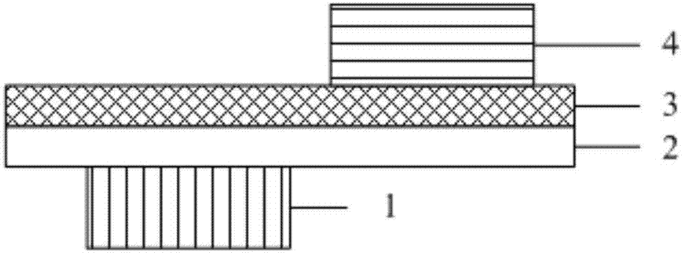
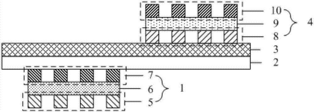
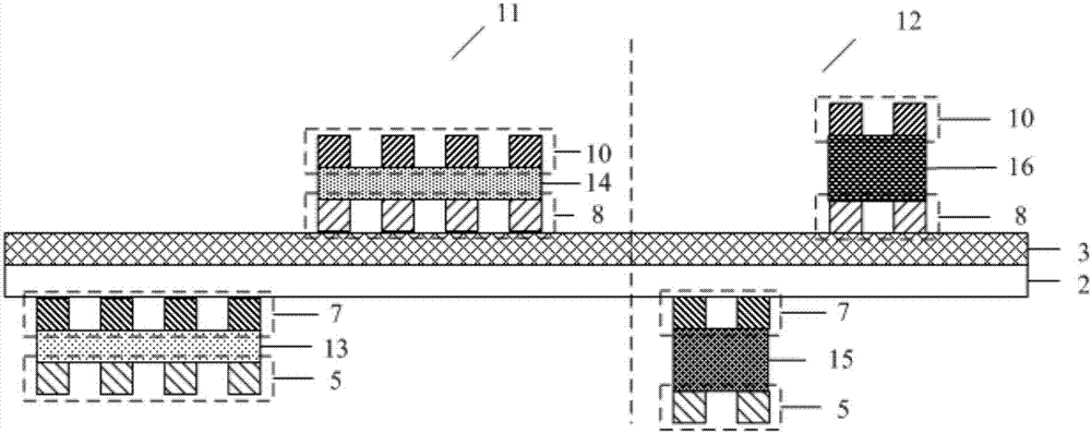
[0041] An array substrate provided in an embodiment of the present application, such as figure 1As shown, the array substrate includes: an ultrasonic emission sensor 1, a glass substrate 2 above the ultrasonic emission sensor 1, a thin film transistor TFT pixel circuit layer 3 on the glass substrate 2, and a thin film transistor TFT pixel circuit layer 3 on the TFT pixel circuit The ultrasonic receiving sensor 4 electrically connected to the TFT pixel circuit layer 3 on the layer 3; wherein, the projections of the ultrasonic transmitting sensor 1 and the ultrasonic receiving sensor 4 in the direction perpendicular to the glass substrate do ...


PUM


Abstract

The invention provides an array substrate, a display panel, a display device and a preparation method for the array substrate and is used for integrating a gesture identification and/or fingerprint identification ultrasonic sensor and the array substrate. According to the array substrate, on the basis of realizing a display function, gesture identification and/or fingerprint identification can be realized, so an application additional value of the array substrate is increased. The array substrate provided by the embodiment of the invention comprises an ultrasonic transmitting sensor, a glass substrate on the ultrasonic transmitting sensor, a thin film transistor TFT pixel circuit layer on the glass substrate, and an ultrasonic receiving sensor which is arranged on the TFT pixel circuit layer and is electrically connected with the TFT pixel circuit layer, wherein projections of the ultrasonic transmitting sensor and the ultrasonic receiving sensor vertical to the direction of glass substrate are not overlapped.

Description

technical field [0001] The present application relates to the field of display, and in particular to an array substrate, a display panel, a display device and a method for preparing the array substrate. Background technique [0002] In the prior art, a micro-electro-mechanical system (MEMS) array of silicon-based ultrasonic transducers is used to send and receive ultrasonic waves, detect gesture positions, and perform gesture recognition. Display device integrated gesture recognition is based on the module integration of silicon-based MEMS array and complementary metal oxide semiconductor integrated circuit (Complementary Metal Oxide Semiconductor Integrated Circuit, CMOS IC). [0003] To sum up, in the prior art, the functional modules for realizing gesture recognition are completely external, and are not integrated with the display screen. Contents of the invention [0004] Embodiments of the present application provide an array substrate, a display panel, a display dev...

Claims


Application Information

Patent Timeline
IPC IPC(8): G06F3/043G06F3/0488G06F3/041
CPCG06F3/0412G06F3/043G06F3/04883G06F2203/04103H01L27/1214G06V40/1306H10N30/302H10N30/87
Inventor 韩艳玲董学王海生吴俊纬丁小梁刘英明郭玉珍郑智仁李昌峰
Owner BOE TECH GRP CO LTD
Why Eureka
Try Eureka