High speed rigid-flexible PCB design method

A technology of soft and hard combination board and design method, which is applied in the direction of computer design circuit, printed circuit making wiring diagram, electrical components, etc., which can solve the problems of signal reflection, failure to consider the impact of impedance, and damage to signal integrity, etc., to avoid crosstalk , to avoid reflection effects

Active Publication Date: 2017-07-18
P C B A ELECTRONICS WUXI
View PDF5 Cites 4 Cited by
  • Summary
  • Abstract
  • Description
  • Claims
  • Application Information

AI Technical Summary

Problems solved by technology

In this way, although the impedance matching between the hard area and the soft area is guaranteed, the line width and spacing changes in the soft-hard transition area will cause signal reflection, and the impedance influence between multiple monoliths when the flexible area is bent has not been considered.
There are multiple flexible boards with a single piece of soft board. When the soft board is bent in the same direction, due to the thickness of the board and the gap between layers, the outermost soft board will be stretched and the innermost soft board will

Method used


Image

  • High speed rigid-flexible PCB design method
  • High speed rigid-flexible PCB design method
  • High speed rigid-flexible PCB design method

Examples


Embodiment Construction

[0028] The present invention will be further described below in conjunction with drawings and embodiments. It should be understood that the specific embodiments described here are only used to explain the present invention, but not to limit the present invention. In addition, it should be noted that, for the convenience of description, only some parts related to the present invention are shown in the accompanying drawings but not the whole content. Unless otherwise defined, all technical and scientific terms used herein are related to the technical field of the present invention. The skilled person generally understands the same meaning. The terms used herein are for describing specific embodiments only, and are not intended to limit the present invention.

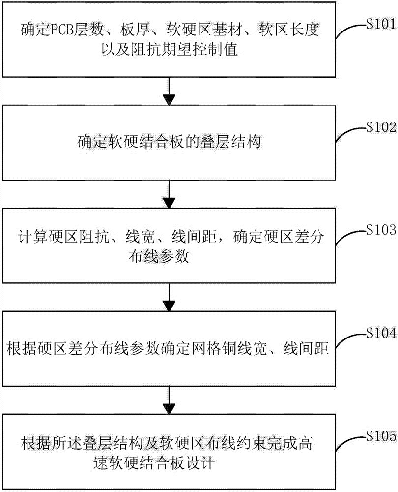
[0029] Please refer to figure 1 as shown, figure 1 It is a flow chart of the high-speed rigid-flex board design method provided by the embodiment of the present invention.

[0030] The design method of the high-speed r...


PUM


Abstract

The invention discloses a high speed rigid-flexible PCB design method. The high speed rigid-flexible PCB design method comprises steps that S101, a number of layers, thickness, base materials of a flexible region and a rigid region, a length of a flexible region, and an impedance expected control value are determined; S102, the laminated structure of the rigid-flexible PCB is determined; S103, impedance, a line width, and a line interval of a rigid region are calculated, and the difference wiring parameters of the rigid region are determined; S104, a grid copper wire width and the line width are determined according to the difference wiring parameters of the rigid region; S105, the design of the high speed rigid-flexible PCB is completed according to the laminated structure and rigid-flexible region wiring constraints. By adopting the reasonable laminated structure, a mutual influence problem of adjacent single chip impedances caused by the bending of the flexible region of the rigid-flexible PCB is solved, and the grid copper wires are used to constrain the wiring parameters of the flexible region and the rigid region to be consistent with each other, and reflection caused by a variable wire width of a flexible-rigid transition region is prevented; by controlling intervals among the high speed signal lines of the flexible region, signal integrity is prevented from being damaged by crosstalk between the high speed signal lines.

Description

technical field [0001] The invention relates to the field of rigid-flex boards, in particular to a design method for high-speed rigid-flex boards. Background technique [0002] Rigid-flex boards have been widely used in products such as consumer electronics, communications, industrial control, and national defense because of their advantages of being bendable and light in weight, and have become an important branch of circuit board development. Rigid-flex board is obtained by pressing the flexible board and the hard board, and then opening the window in the flexible area of ​​the hard board. In recent years, mass-produced digital products require timing control at the picosecond level. These timing levels need to be maintained not only at the silicon level, but also on a physically larger system board, such as a computer motherboard. The operating frequency of these systems is very high, and the behavior of the wire is no longer like a simple ideal wire, but will show high...

Claims


Application Information

Patent Timeline
IPC IPC(8): H05K3/00
CPCH05K3/0002H05K3/0005H05K2201/0776
Inventor 王永康吉中娟陈懿肖如全赵飞赵翔
Owner P C B A ELECTRONICS WUXI
Why Eureka
Try Eureka