Inclined metal nano-structure and preparation method thereof
A metal nanostructure and metal technology, which is applied in the preparation of test samples, metal material coating process, ion implantation plating, etc., can solve the problems of difficult preparation process of inclined metal nanostructures, limited effective area of samples, time-consuming and labor-intensive, etc. , to achieve the effect of convenient optical detection, time saving and strong controllability
- Summary
- Abstract
- Description
- Claims
- Application Information
AI Technical Summary
Problems solved by technology
Method used
Image
Examples
Embodiment 1
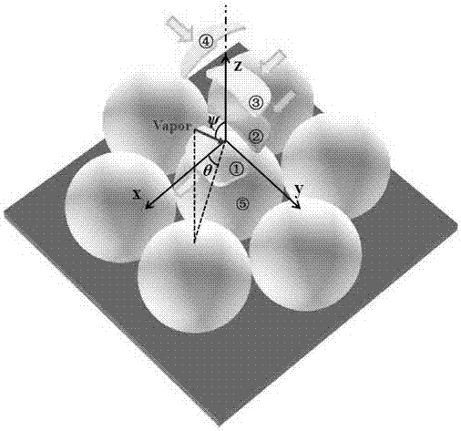
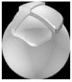
[0042] Such as figure 2 The tilted silver nanostructure shown, deposited on the surface of a polystyrene sphere, consists of a first silver layer, a silicon dioxide layer, a second silver layer, and a third silver layer, the first silver layer and the silicon dioxide The layers are all deposited on the surface of polystyrene pellets, and the first silver layer and the silicon dioxide layer are butted together, and the second silver layer is deposited on the upper surface of the silicon dioxide layer; the third silver layer is perpendicular to the second silver layer and the first silver layer, and the third silver layer is deposited on the upper surface upper ends of the first silver layer and the second silver layer;
[0043]The thicknesses of the first silver layer, the second silver layer and the third silver layer are the same, and the thickness of the silicon dioxide layer is greater than that of the first silver layer, the second silver layer and the third silver layer....
Embodiment 2
[0063] The difference between the preparation method of this example and Example 1 is that the deposition time of silicon dioxide is 600 s, and the rest are the same as Example 1.
[0064] Put the structure obtained in this embodiment into a cuvette, and measure its circular dichroism signal by normal incidence in a circular dichroism spectrometer, and obtain the following: Figure 5 The deposition time of the insulating material is the curve of 600s.
Embodiment 3
[0066] The difference between the preparation method of this example and Example 1 is that the deposition time of silicon dioxide is 700s, and the rest are the same as Example 1.
[0067] Put the structure obtained in this embodiment into a cuvette, and measure its circular dichroism signal by normal incidence in a circular dichroism spectrometer, and obtain the following: Figure 5 The deposition time of medium insulating material is 700s curve.
PUM
| Property | Measurement | Unit |
|---|---|---|
| diameter | aaaaa | aaaaa |
Abstract
Description
Claims
Application Information


