Back electrode structured impurity barrier band detector and manufacturing method therefor

A technology to block impurities and back electrodes, applied in the direction of final product manufacturing, sustainable manufacturing/processing, circuits, etc., can solve problems such as damage, and achieve the effects of avoiding difficult operation, improving yield, and reducing dark current

Active Publication Date: 2017-08-04
NO 50 RES INST OF CHINA ELECTRONICS TECH GRP
View PDF3 Cites 14 Cited by
  • Summary
  • Abstract
  • Description
  • Claims
  • Application Information

AI Technical Summary

Problems solved by technology

The negative electrode and the metal substrate are bonded together with silver glue, and the gold wires are respectively drawn out from the positive electrode and the metal substrate through the wire bonding process, and connected to the adjacent pins of the metal substrate respectively, avoiding the need for deep hole engraving in the traditional preparation method Etching the negative electrode solves the problem of damage to the device caused by the traditional etching process, and can reduce the dark current; at the same time, the preparation of the device with the back electrode structure avoids the difficulty in the operation of drawing gold wires from the micropores in the traditional packaging method, and improves the efficiency of the device. negative electrode yield

Method used


Image

  • Back electrode structured impurity barrier band detector and manufacturing method therefor
  • Back electrode structured impurity barrier band detector and manufacturing method therefor
  • Back electrode structured impurity barrier band detector and manufacturing method therefor

Examples


Embodiment Construction

[0055] The present invention will be described in detail below in conjunction with specific embodiments. The following examples will help those skilled in the art to further understand the present invention, but do not limit the present invention in any form. It should be noted that those skilled in the art can make several changes and improvements without departing from the concept of the present invention. These all belong to the protection scope of the present invention.

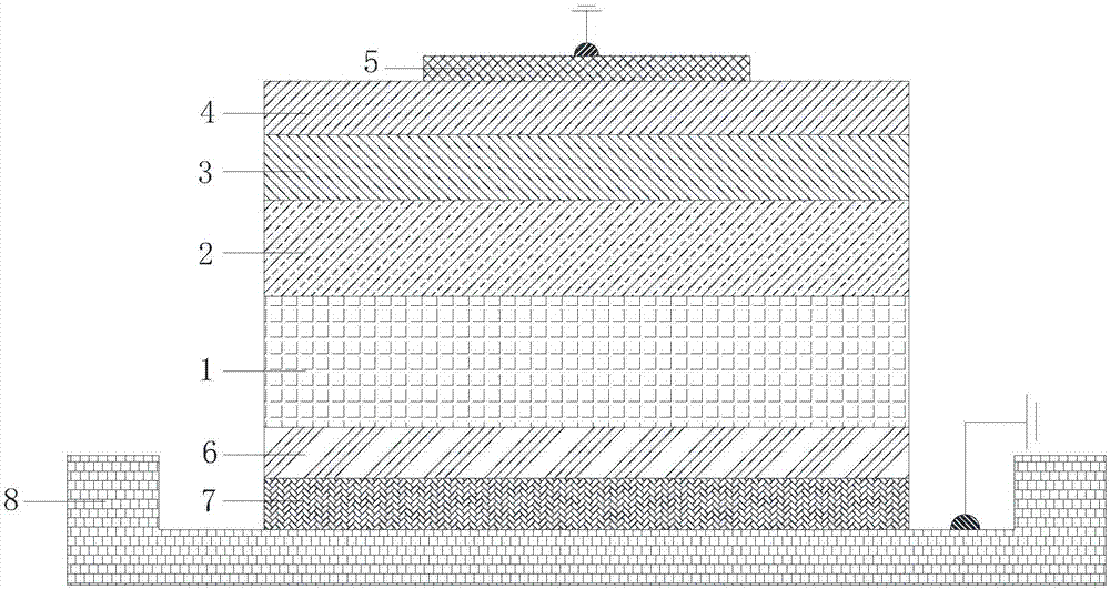
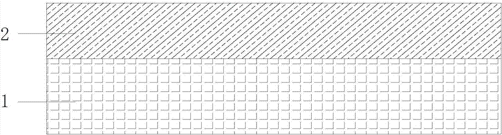
[0056] Such as Figure 1 to Figure 7 As shown, the high-conductivity silicon substrate 1 used in the barrier impurity band detector of the back electrode structure of the present invention is doped with arsenic ions, and the doping concentration is 2×10 19 cm -3 , with a thickness of 450 μm; a silicon-phosphorus-doped epitaxial layer was grown on a highly conductive silicon substrate 1 by chemical vapor deposition as the absorber layer 2, with a thickness of 30 μm and a doping concentration of 5×10 17...


PUM


Abstract

The invention provides a back electrode structured impurity barrier band detector. The back electrode structured impurity barrier band detector comprises a high-conductivity silicon substrate, a silicon-doped phosphorus absorption layer, a high-purity silicon barrier layer, an electrode transitional region, a positive electrode region, a negative electrode region and a metal substrate, wherein the silicon-doped phosphorus absorption layer is arranged on the high-conductivity silicon substrate; the high-purity silicon barrier layer is arranged on the silicon-doped phosphorus absorption layer; the electrode transitional region is arranged on the high-purity silicon barrier layer; the positive electrode region is arranged on the electrode transitional region; a positive electrode lead is arranged on the positive electrode region; the negative electrode region is arranged at the bottom of the high-conductivity silicon substrate; the negative electrode region is connected with the metal substrate through conductive silver paste; and a negative electrode lead is arranged on the negative electrode region. The back electrode structured impurity barrier band detector has the beneficial effects as follows: the negative electrode and the metal substrate are glued together through the silver paste; gold lines are led from the positive electrode and the metal substrate separately through a lead bonding process to be connected to adjacent pins of the metal substrate respectively; and therefore, deep hole etching to the negative electrode in the conventional preparation method is avoided, and the problem of damage to the device caused by the conventional etching process is solved.

Description

technical field [0001] The invention relates to a preparation process and packaging method of a detector, in particular to a preparation and packaging method of a blocking impurity strip detector with a back electrode structure, which is suitable for making a blocking impurity strip detector with low dark current and high response rate. Background technique [0002] The working band of the silicon-based barrier impurity band detector is 5 μm to 40 μm, which can realize the detection of very long wave to terahertz band. Its working mechanism is as follows: a thin intrinsic barrier layer is grown on the heavily doped absorbing layer to effectively suppress the dark current generated by the impurity energy band. The incident terahertz radiation directly passes through the barrier layer and is absorbed by the absorbing layer, which excites the electrons on the impurity band to transition to the conduction band. After the transition, the electrons are collected by the positive el...

Claims


Application Information

Patent Timeline
Patent Type & Authority Applications(China)
IPC IPC(8): H01L31/09H01L29/06H01L31/18
CPCH01L29/0603H01L29/0684H01L31/09H01L31/1876Y02P70/50
Inventor 陈雨璐王晓东王兵兵潘鸣侯丽伟谢巍臧元章张传胜周德亮
Owner NO 50 RES INST OF CHINA ELECTRONICS TECH GRP
Why Eureka
Try Eureka