
A Method for Calculating Channel Capacity and Imaging Error Lower Limit of Coherent Imaging Lithography System

A technology of channel capacity and imaging error, which is applied in the fields of microelectronics manufacturing and information theory, and can solve problems such as difficulty in solving the theoretical lower limit of channel capacity and imaging error of lithography system.

Active Publication Date: 2018-04-10
BEIJING INSTITUTE OF TECHNOLOGYGY
View PDF3 Cites 0 Cited by
  • Summary
  • Abstract
  • Description
  • Claims
  • Application Information

AI Technical Summary

Problems solved by technology

The nonlinear characteristics of the imaging model of the lithography system and the diversity of the circuit layout make it difficult to solve the theoretical lower limit of the channel capacity and imaging error of the lithography system. At present, there is no specific calculation method for the theoretical lower limit of the channel capacity and imaging error of the lithography system.

Method used


Image

  • A Method for Calculating Channel Capacity and Imaging Error Lower Limit of Coherent Imaging Lithography System
  • A Method for Calculating Channel Capacity and Imaging Error Lower Limit of Coherent Imaging Lithography System
  • A Method for Calculating Channel Capacity and Imaging Error Lower Limit of Coherent Imaging Lithography System

Examples


Embodiment

[0080] Figure 5 501 is a mask of parallel vertical lines, Figure 5 502 is the photoresist image obtained by using the mask in 501, and its imaging error is PE=736. Using the OPC method to Figure 5 The mask in 501 is optimized, and the optimized mask obtained is as follows Figure 5 Shown in 503. Figure 5 504 is used Figure 5 The imaging error of the photoresist obtained by the 503 mask is PE=20. Figure 6 601 is a T-shaped mask, Figure 6 602 is the photoresist imaging obtained by using the mask in 601, and its imaging error is PE=748. Using the OPC method to Figure 6 The mask in 601 is optimized, and the optimized mask obtained is as follows Figure 6 Shown in 603. Figure 6 604 is the photoresist image obtained by using the mask in 603, and its imaging error is PE=98. Depend on Figure 5 and Figure 6 It can be seen that using the OPC method to optimize the mask can compensate the optical proximity effect, thereby further improving the imaging accuracy of t...


PUM


Abstract

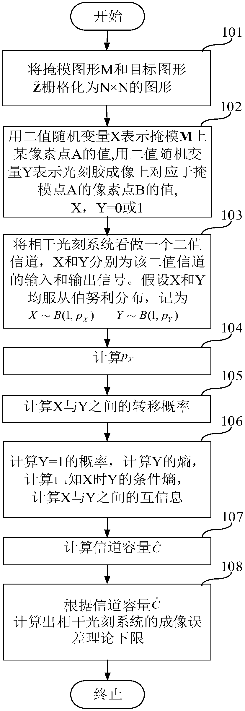
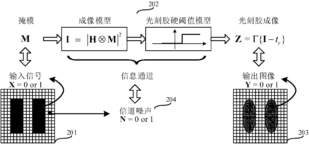
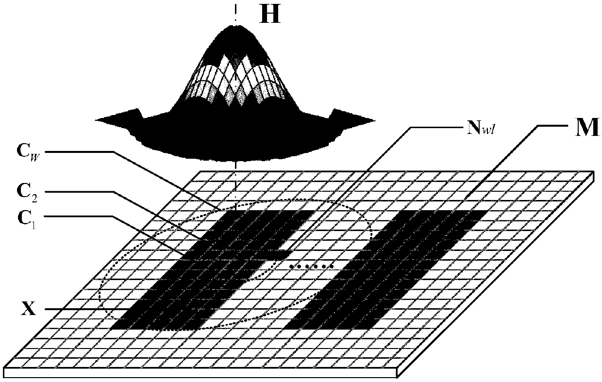
The invention relates to a method for calculating channel capacity and imaging error lower limit of a coherent imaging photoetching system. The method comprises the steps of rasterizing a mask pattern M; expressing a value of a pixel point A on a mask image M with a binary random variable X, and expressing a value of a pixel point B, corresponding to the pixel point A, on a photoresist image Z with a binary random variable Y; viewing the coherent photoetching system as a binary channel, wherein the X and the Y are respectively an input signal and an output signal of the binary channel; calculating probability pX when the X is equal to 1; calculating transfer probability pij between the X and the Y; calculating probability pY when the Y is equal to 1, and further calculating mutual information I (X; Y) between the X and the Y; taking the maximum value C-bar of the mutual information as the channel capacity; and calculating an image error theoretical lower limit of the coherent photoetching system according to the channel capacity C-bar. By the method, a theoretical basis and a simulation basis can be provided for deeper understanding of an image information transmission mechanism and development of an advanced calculation photoetching technology in the photoetching system.

Description

technical field [0001] The invention provides a method for calculating the channel capacity and lower limit of imaging error of a coherent imaging lithography system (hereinafter referred to as "coherent lithography system"), belonging to the technical fields of microelectronics manufacturing and information theory. Background technique [0002] Photolithography is a key technology in the manufacture of integrated circuits. The lithography system irradiates the mask evenly with a certain lighting method and energy, and forms a diffraction field carrying the mask layout information, and then projects the image onto the surface of the semiconductor substrate coated with photoresist through the lithography projection objective lens. This process transfers the structural pattern of an integrated circuit device from a mask to the surface of a silicon wafer or other semiconductor substrate. [0003] However, the interference and diffraction of light will cause optical proximity e...

Claims


Application Information

Patent Timeline
Patent Type & Authority Patents(China)
IPC IPC(8): G03F7/20
CPCG03F7/705
Inventor 马旭张昊王志强李艳秋沈诗欢
Owner BEIJING INSTITUTE OF TECHNOLOGYGY
Learn More