A vertical high-voltage power bipolar junction transistor and its manufacturing method
A technology of bipolar junction type and manufacturing method, which is applied in semiconductor/solid-state device manufacturing, semiconductor devices, electrical components, etc., can solve the problems of withstand voltage, leakage and gain, frequency, and device size that are difficult to reconcile, and achieve the reduction of curvature effect , BVceo improved effect
- Summary
- Abstract
- Description
- Claims
- Application Information
AI Technical Summary
Problems solved by technology
Method used
Image
Examples
Embodiment 1
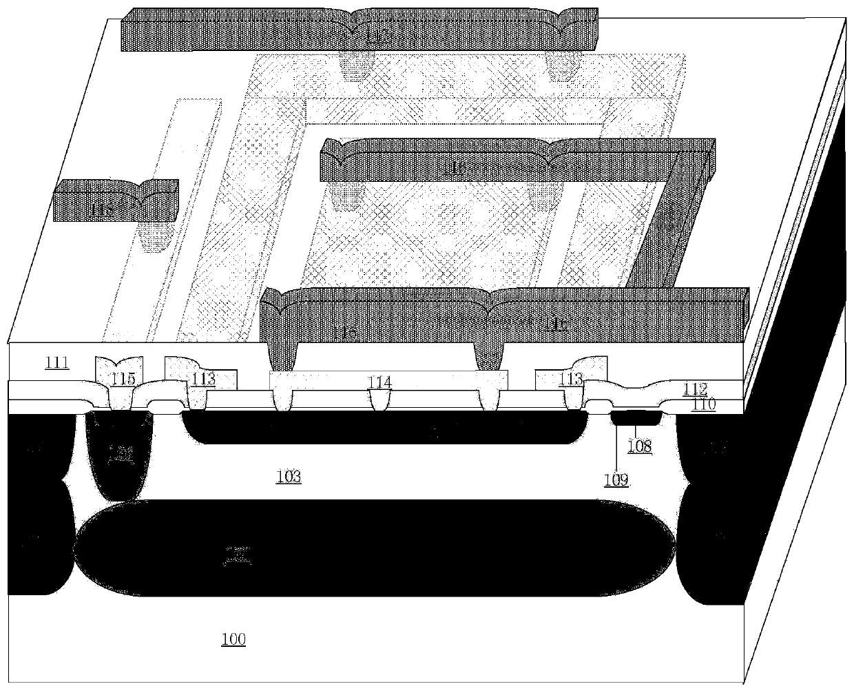
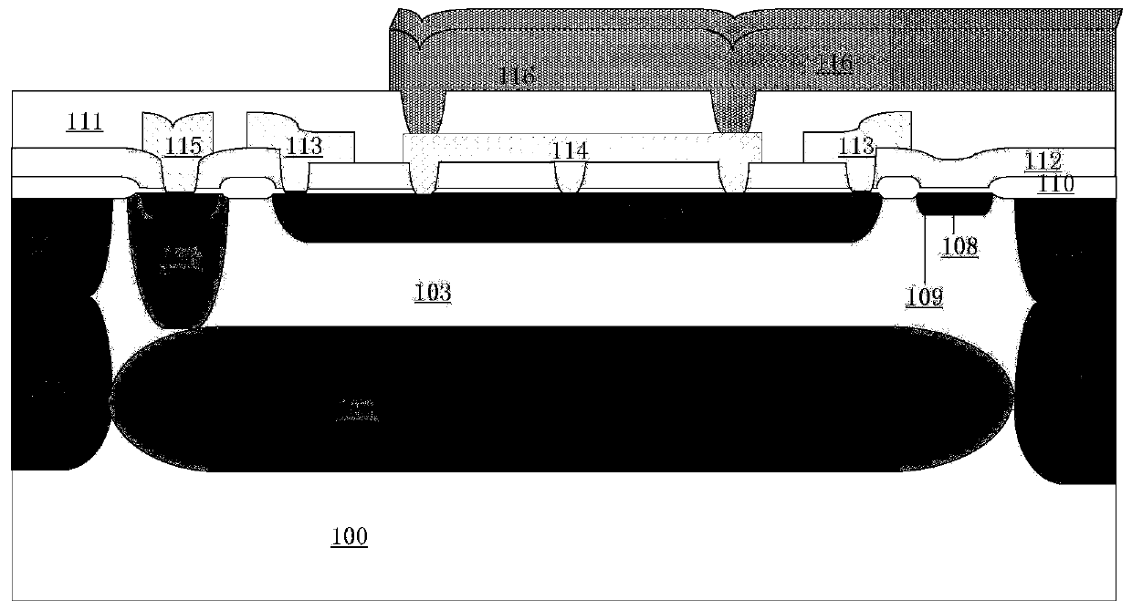
[0067] Such as figure 1 with figure 2 , A vertical high voltage power bipolar junction transistor, characterized in that it comprises a P-type substrate 100, an N-type buried layer 101, a P-type buried layer 102, an N-type epitaxial layer 103, a P-type base region 104, and a P-type isolation Through region 105, N-type through region 106, N-type heavily doped emitter region 107, N-type heavily doped ring-shaped collector region 108, pre-oxygen layer 109, field oxygen layer 110, IMD planarization dielectric 111, TEOS metal Front dielectric layer 112, base first layer metal 113, emitter first layer metal 114, collector first layer metal 115, emitter second layer metal 116, base second layer metal 117, and collector second layer Metal 118.
[0068] The N-type buried layer 101 is located in the middle of the upper surface of the P-type substrate 100.
[0069] The P-type buried layer 102 is located on two sides of the upper surface of the P-type substrate 100.
[0070] The N-type epitax...
Embodiment 2
[0088] Such as Figure 3 ~ Figure 13 As shown, a method for manufacturing a vertical high-voltage power bipolar junction transistor is characterized in that it includes the following steps:
[0089] 1) Choose NTD with fewer defects Single chip, thickness of about 500~700μm, resistivity of 5~30Ω·cm, marking, cleaning and drying for later use;
[0090] 2) Grow a thick oxide layer Temperature 1100~1150℃, time 100min~120min, dry humidification and oxidation conditions.
[0091] 3) One photolithography, after photolithography and etching, grow a thin oxide layer Temperature 1000~1020℃, time 30min~40min, pure dry oxidation conditions.
[0092] The N-type buried layer 101 is implanted in the middle of the wafer substrate, and the ion implantation conditions are: dose 1e15~5e15cm -2 , Energy 40~80KeV.
[0093] The redistribution conditions are: aerobic conditions of 1000 ℃, the thickness of the oxide layer Re-annealing temperature pure N 2 , 1100~1150℃, time 100min~120min.
[0094] 4) The s...
PUM
| Property | Measurement | Unit |
|---|---|---|
| thickness | aaaaa | aaaaa |
| electrical resistivity | aaaaa | aaaaa |
| thickness | aaaaa | aaaaa |
Abstract
Description
Claims
Application Information


