A vertical high-voltage bipolar junction transistor and its manufacturing method
A bipolar junction and transistor technology, which is applied in transistors, semiconductor/solid-state device manufacturing, semiconductor devices, etc., can solve problems such as difficulty in reconciling parameters such as withstand voltage and gain, frequency, and device size of bipolar junction devices. , to achieve the effect of simple and feasible structure
- Summary
- Abstract
- Description
- Claims
- Application Information
AI Technical Summary
Problems solved by technology
Method used
Image
Examples
Embodiment 1
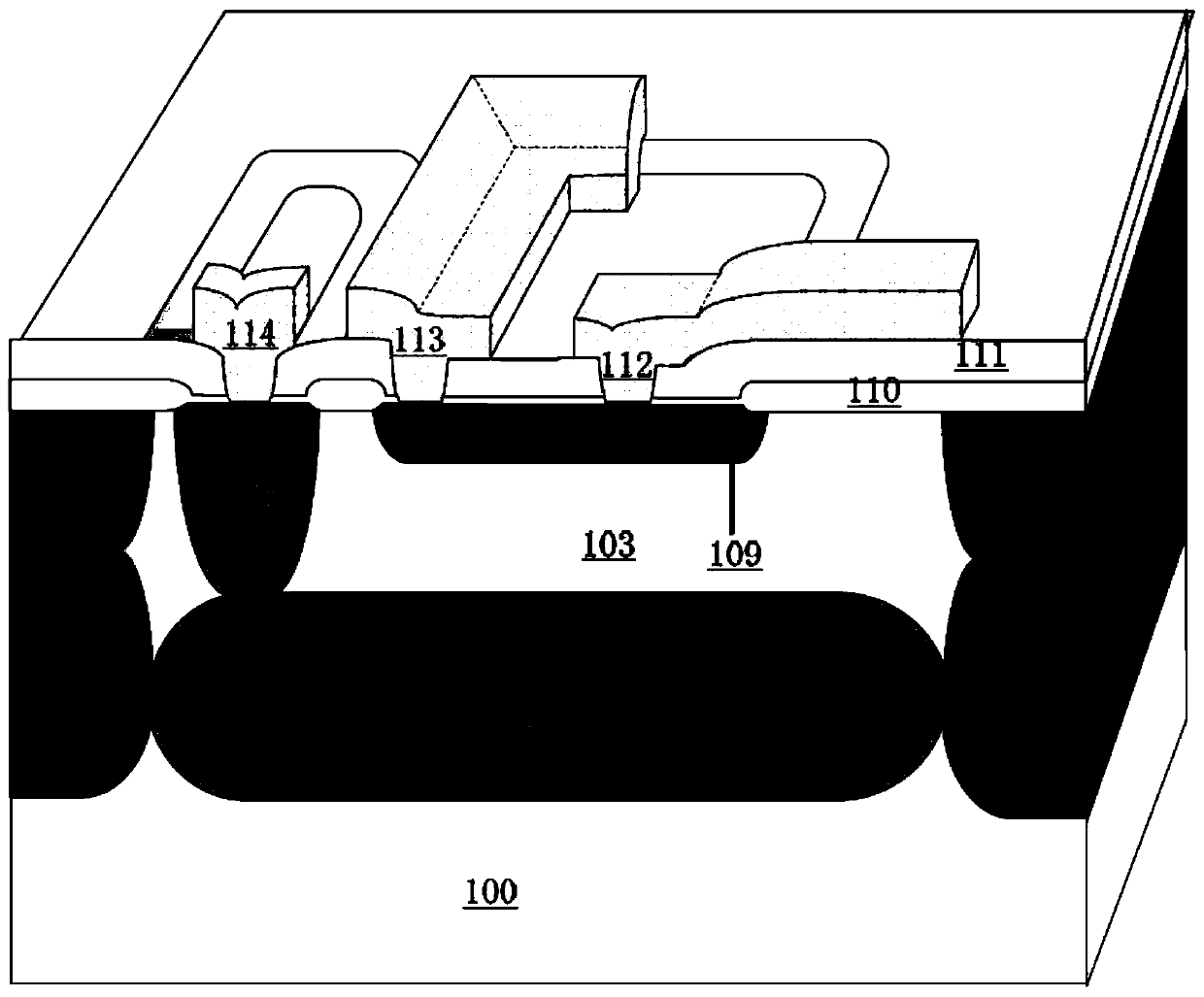
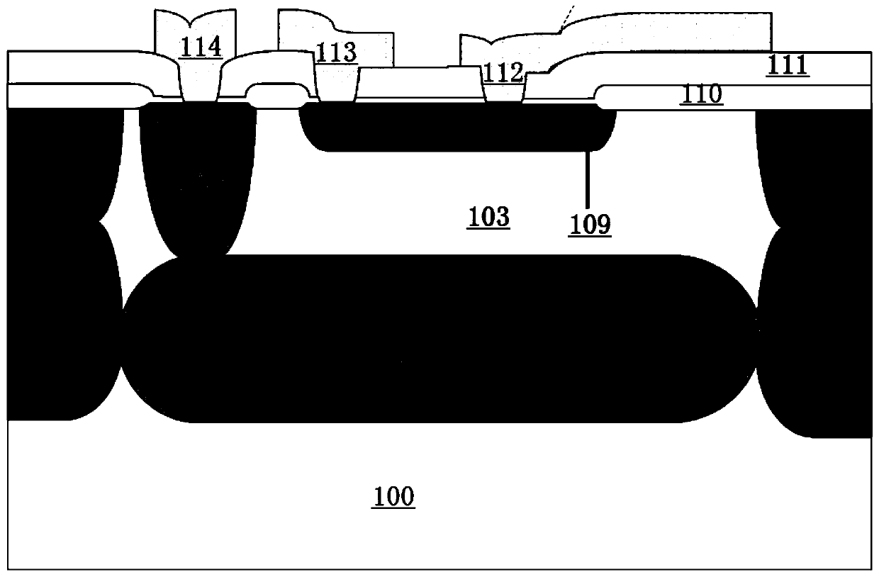
[0059] A vertical high voltage bipolar junction transistor is characterized by comprising a P-type substrate 100, an N-type buried layer 101, a P-type buried layer 102, an N-type epitaxial layer 103, an N-type heavily doped emitter region 104, a P-type Isolation penetration region 105, N-type through region 106, P-type base region 107, N-type heavily doped collector region 108, pre-oxide layer 109, field oxide layer 110, TEOS metal front dielectric layer 111, emitter metal 112, Collector metal 114 and base metal 113.
[0060] The N-type buried layer 101 is located at the center of the upper surface of the P-type substrate 100 .
[0061] The P-type buried layer 102 is located at both ends of the upper surface of the P-type substrate 100 .
[0062] The N-type epitaxial layer 103 is located on the N-type buried layer 101 , and the N-type epitaxial layer 103 is in contact with the P-type substrate 100 , the N-type buried layer 101 and the P-type buried layer 102 .
[0063] The P...
Embodiment 2
[0075] like Figure 3 to Figure 11 As shown, a method for manufacturing a vertical high-voltage bipolar junction transistor is characterized by comprising the following steps:
[0076] 1) Select the NTD single wafer with fewer defects, the thickness of the wafer is about 500-700μm, the resistivity is 5-30Ω·cm, marking, cleaning and drying are used;
[0077] 2) grow a thick oxide layer Temperature 1100 ~ 1150 ℃, time 100min ~ 120min, dry humidification oxidation conditions.
[0078] 3) One photolithography, after photolithography is removed, a thin oxide layer is grown Temperature 1000~1020℃, time 30min~40min, pure dry oxidation conditions.
[0079] The N-type buried layer 101 is implanted in the middle of the wafer substrate, and the ion implantation conditions are: dose 1e15~5e15cm -2 , Energy 40 ~ 80KeV.
[0080] The redistribution conditions are: aerobic conditions of 1000 °C, and the thickness of the oxide layer is Re-annealing temperature is pure N2, 1100~1150℃, ...
PUM
| Property | Measurement | Unit |
|---|---|---|
| thickness | aaaaa | aaaaa |
| electrical resistivity | aaaaa | aaaaa |
| thickness | aaaaa | aaaaa |
Abstract
Description
Claims
Application Information


