High-voltage substrate PNP bipolar junction type transistor and manufacturing method thereof
A technology of bipolar junction type and manufacturing method, which is applied in the direction of transistor, semiconductor/solid-state device manufacturing, semiconductor device, etc., can solve the difficulties, the parameters such as withstand voltage and gain, frequency, and device size of bipolar junction devices are difficult to reconcile, etc. problem, to achieve the effect of simple and feasible structure
- Summary
- Abstract
- Description
- Claims
- Application Information
AI Technical Summary
Problems solved by technology
Method used
Image
Examples
Embodiment 1
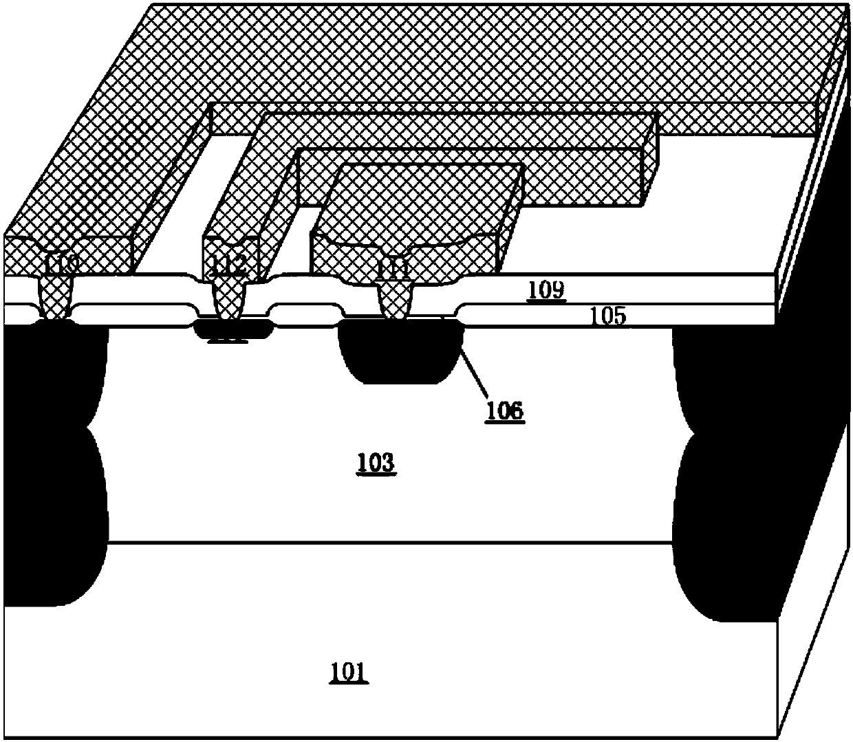
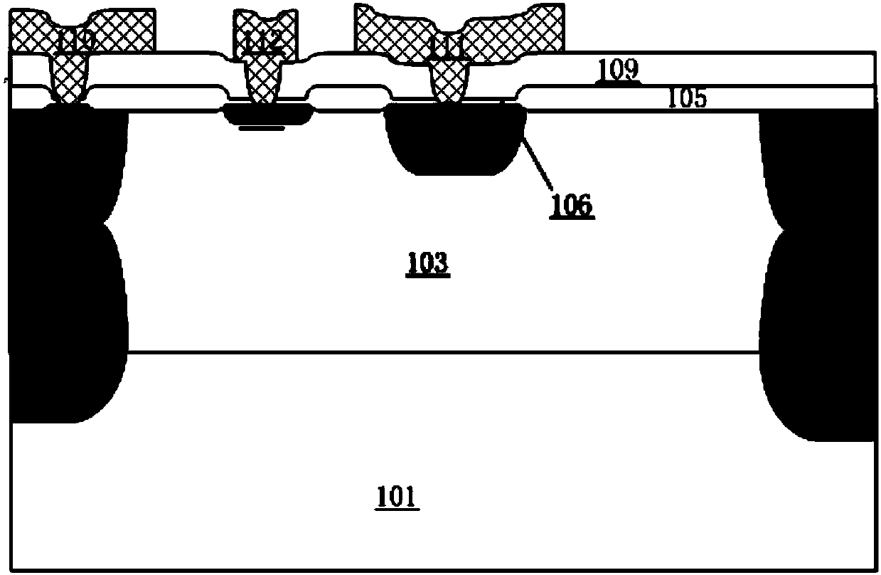
[0053] Such as figure 1 with figure 2 As shown, a high-voltage substrate PNP bipolar junction transistor is characterized in that it includes: a P-type substrate 101, a P-type buried layer 102, an N-type epitaxial layer 103, a P-type isolation penetration region 104, and a field oxygen layer 105, pre-oxidation layer 106, P-type emitter / collector region 107, N-type heavily doped base region 108, TEOS metal front dielectric layer 109, first layer metal 110 in collector region, first layer metal 111 in emitter region and Base first layer metal 112 .
[0054] The P-type buried layer 102 covers both ends of the upper surface of the P-type substrate 101 .
[0055] The N-type epitaxial layer 103 covers part of the surface on the P-type substrate 101 . The N-type epitaxial layer 103 is in contact with the P-type buried layer 102 .
[0056] The P-type isolation penetration region 104 covers the P-type buried layer 102 . The P-type isolation penetration region 104 is in contact with...
Embodiment 2
[0070] Such as Figure 3 to Figure 9 Shown, a kind of manufacturing method of high voltage substrate PNP bipolar junction transistor is characterized in that, comprises the following steps:
[0071] 1) Select a NTD single chip with less defects, with a thickness of about 500-700 μm and a resistivity of 5-30Ω·cm, marking, cleaning, and drying for later use;
[0072] 2) Growth of a thick oxide layer Temperature 1100~1150℃, time 100min~120min, dry humidification oxidation conditions.
[0073] 3) One photolithography, after photolithography etch to remove glue, grow a thin oxide layer Temperature 1000~1020℃, time 30min~40min, pure dry oxidation conditions.
[0074] Implant the P-type buried layer 102 at both ends of the wafer substrate, and the ion implantation conditions are: dose 4e15-8e15cm -2 , Energy 60 ~ 100KeV.
[0075] The redistribution condition is: pure N 2 Atmospheric annealing temperature, 1100-1150°C, time 100min-120min. Remove the oxide layer.
[0076] 4) ...
PUM
| Property | Measurement | Unit |
|---|---|---|
| Thickness | aaaaa | aaaaa |
| Resistivity | aaaaa | aaaaa |
| Thickness | aaaaa | aaaaa |
Abstract
Description
Claims
Application Information


