Method for transferring silver nanowire transparent conductive film to flexible substrate
A technology of transparent conductive film and silver nanowires, which can be used in the manufacture of conductive/semiconductive layers of equipment, circuits, electrical components, etc. Sensor sensitivity and other issues, the transfer method is simple and easy to operate, low in cost, and the effect of reducing surface roughness
- Summary
- Abstract
- Description
- Claims
- Application Information
AI Technical Summary
Problems solved by technology
Method used
Image

Examples
Embodiment 1
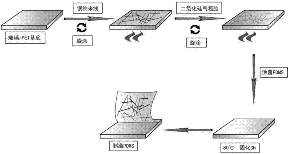
[0032] See attached figure 1 , the present invention comprises the following steps:
[0033] (1) Preparation of silver nanowire transparent conductive film:
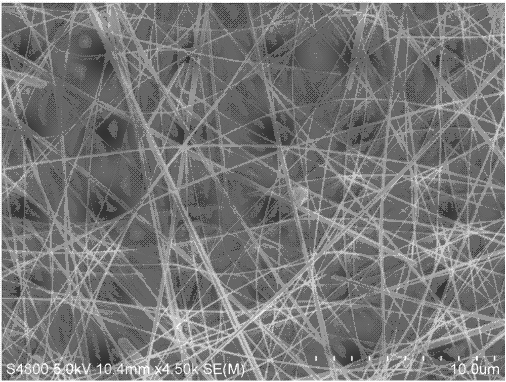
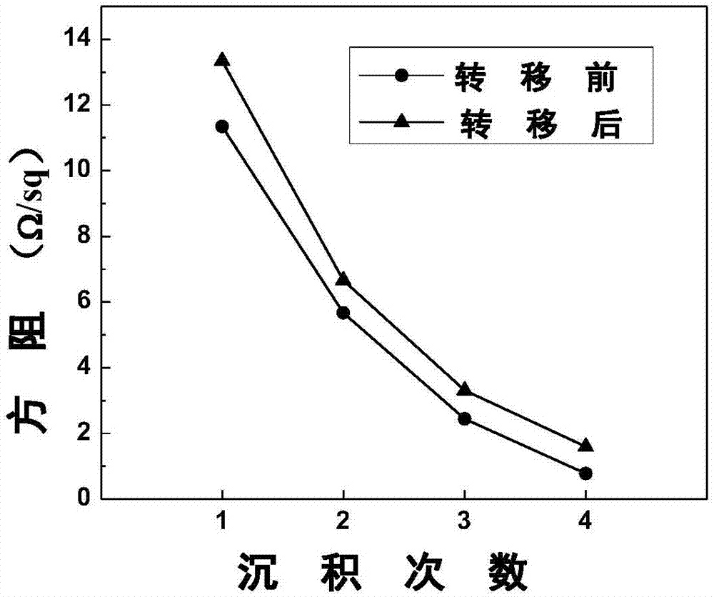
[0034] Add the silver nanowire absolute ethanol dispersion onto a clean glass substrate, spin-coat at a speed of 1200 rpm, deposit a layer of silver nanowire network substrate with a certain arrangement density, and then coat the silver nanowire The glass substrate of the transparent conductive film was placed on a heating plate at 120°C for 10 minutes to obtain a transparent conductive film of silver nanowires. The transmittance at 550nm wavelength was measured to be 81.7% at this time with a UV-visible spectrophotometer. The square resistance measured by the needle is 11.35Ω sq. -1 .
[0035] (2) Preparation of silica airgel / AgNWs composite conductive film:
[0036] Gas-phase nano silicon dioxide is dispersed in 12ml dehydrated alcohol solution with the massfraction of 4ωt%, on the silver nanowire transparent condu...
Embodiment 2
[0039] Embodiment 2: see attached figure 1 , the present invention comprises the following steps:
[0040] (1) Add the silver nanowire absolute ethanol dispersion onto a clean glass substrate, spin-coat at a speed of 1200 rpm, deposit 2 layers of silver nanowire network substrates with a certain arrangement density, and then coat the The glass substrate of the silver nanowire transparent conductive film was placed on a heating plate at 120° C. for 10 minutes to obtain the silver nanowire transparent conductive film. The transmittance at the wavelength of 550 nm was 74.38% when measured by a UV-visible spectrophotometer. The square resistance measured by four probes is 5.67Ω sq. -1 , due to the increase in the number of nanowire depositions and the increase in the silver nanowire network, the transmittance is lower than that in Example 1, while the conductivity is increased.
[0041] (2) gas-phase nano silicon dioxide is dispersed in 12ml dehydrated ethanol solution with the ...
Embodiment 3
[0043] Embodiment 3: see attached figure 1 , the present invention comprises the following steps:
[0044] (1) Add the silver nanowire absolute ethanol dispersion onto a clean glass substrate, spin-coat at a speed of 1200 rpm, deposit 3 layers of silver nanowire network substrates with a certain arrangement density, and then coat the The glass substrate of the silver nanowire transparent conductive film was placed on a heating plate at 120° C. for 10 minutes to obtain the silver nanowire transparent conductive film. The transmittance at 550nm wavelength was 64.96% when measured by a UV-visible spectrophotometer. The square resistance measured by four probes is 2.44Ω sq. -1 , due to the increase in the number of nanowire depositions and the increase in the silver nanowire network, the transmittance is lower than that of Example 2, while the conductivity is increased.
[0045] (2) gas-phase nano silicon dioxide is dispersed in 12ml dehydrated ethanol solution with the mass fra...
PUM
| Property | Measurement | Unit |
|---|---|---|
| Diameter | aaaaa | aaaaa |
| Length | aaaaa | aaaaa |
Abstract
Description
Claims
Application Information
 - R&D
- Intellectual Property
- Life Sciences
- Materials
- Tech Scout
- Unparalleled Data Quality
- Higher Quality Content
- 60% Fewer Hallucinations
Browse by: Latest US Patents, China's latest patents, Technical Efficacy Thesaurus, Application Domain, Technology Topic, Popular Technical Reports.
© 2025 PatSnap. All rights reserved.Legal|Privacy policy|Modern Slavery Act Transparency Statement|Sitemap|About US| Contact US: help@patsnap.com