A Lateral Insulated Gate Bipolar Transistor
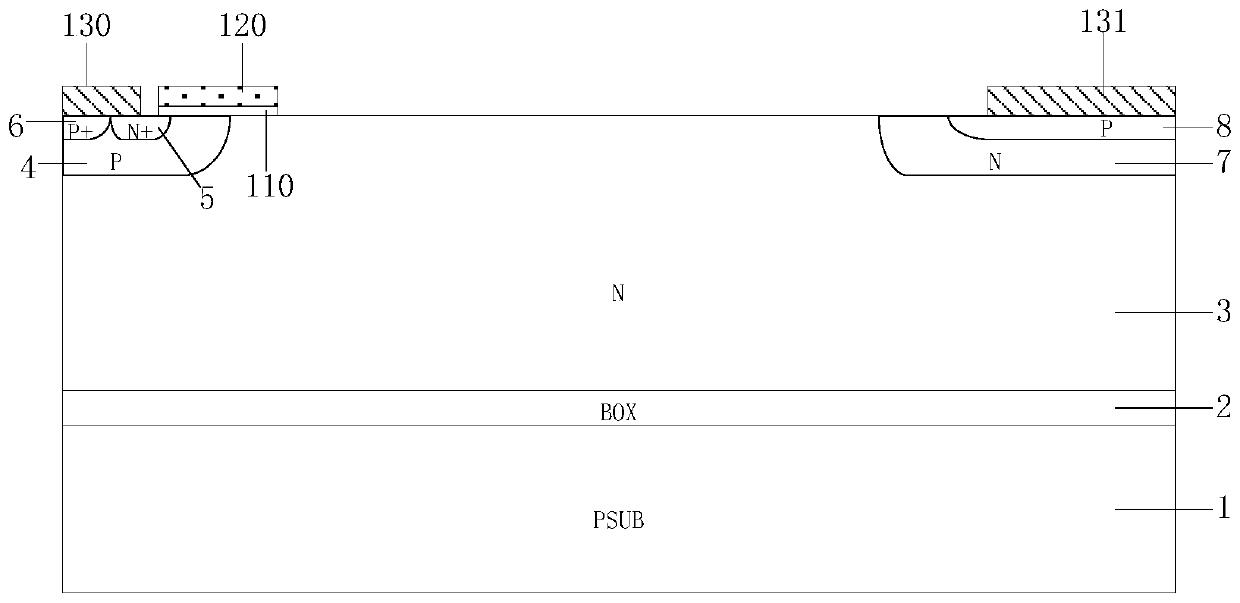
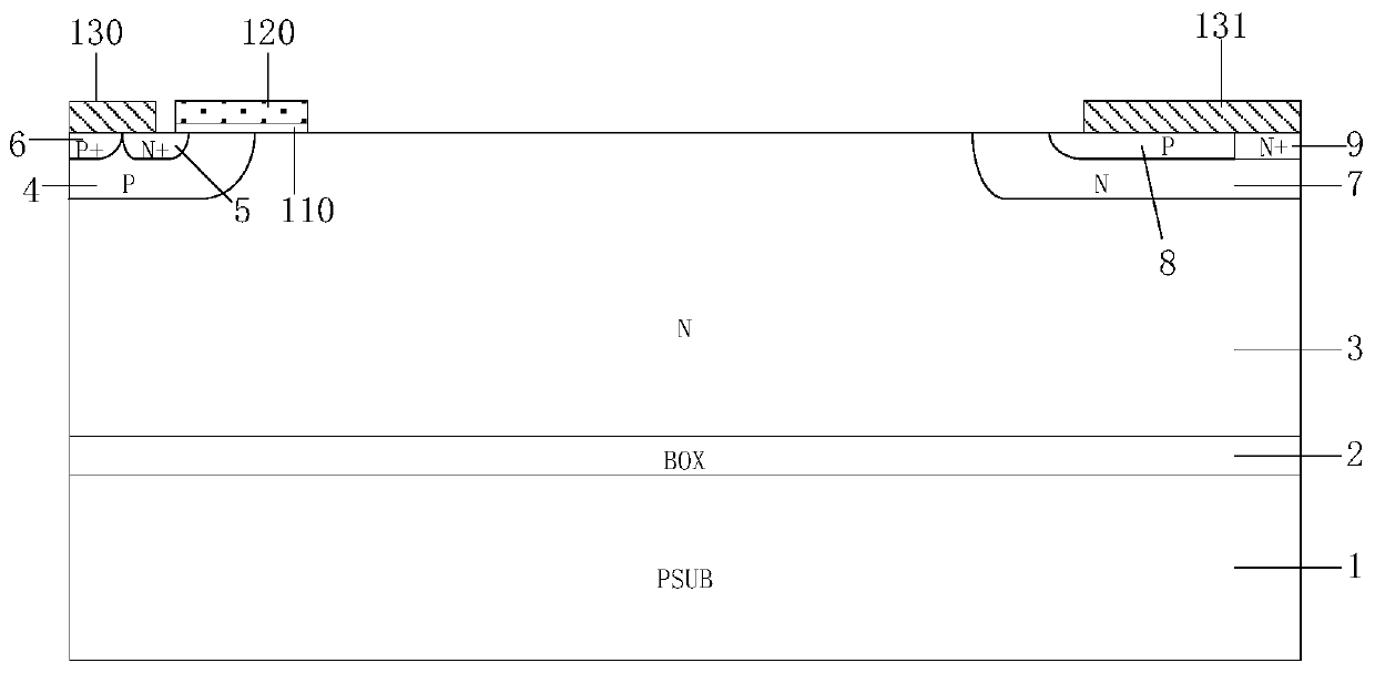
A bipolar transistor, insulated gate technology, applied in transistors, diodes, semiconductor devices, etc., can solve problems such as weakening the conductance modulation effect of the drift region, unfavorable device practical application, increasing forward voltage drop, etc., and achieve high breakdown. Effects of voltage, low turn-off losses, and fast turn-off speed
- Summary
- Abstract
- Description
- Claims
- Application Information
AI Technical Summary
Problems solved by technology
Method used
Image
Examples
Embodiment 1
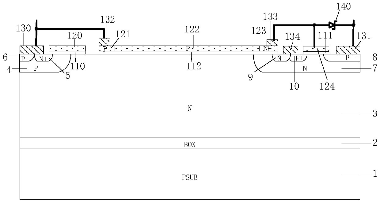
[0030] like image 3 As shown, this is a schematic structural diagram of this example, including a substrate 1, an insulating layer 2 and an N-type low-doping drift region 3 that are sequentially stacked from bottom to top; the upper layer of the N-type low-doping drift region 3 has A P-type body region 4 and an N-type buffer region 7, the upper layer of the P-type body region 4 has a P+ contact region 6 and an N+ emitter region 5 arranged in parallel to each other, wherein the N+ emitter region 5 is located on the side close to the N-type buffer region 7 , the N-type buffer region 7 has a P-type collector region 8; the P+ contact region 6 and part of the N+ emitter region 5 have an emitter metal electrode 130 on the upper surface, and the P-type body region 4 has a first surface on the upper surface. A gate structure, the first gate structure is composed of a first gate dielectric layer 110 and a first polysilicon gate electrode 120 located on the upper surface of the first g...
Embodiment 2
[0037] like Figure 4 As shown, the difference between this embodiment and Embodiment 1 is that in this embodiment, compared with Embodiment 1, the P-type collector region 8 and the collector metal electrode 131 and the highly doped N+ region 9, the highly doped P+ region 10 and The positions of the third metal electrodes 134 are exchanged. Therefore, in this example, the P-type collector region 8 is closer to the P-type body region 4 than the N+ region 9 and the P+ region 10; The thickness of the equivalent N-type buffer layer 7 between 3 further reduces the conduction loss of the device.
Embodiment 3
[0039] like Figure 5As shown, in this embodiment, compared with Embodiment 2, a Zener diode is directly formed in the polysilicon layer above the dielectric layer 112. The Zener diode and the polysilicon diode share the highly doped N+ region 123, and the highly doped N+ region 123 is The anode of the Zener diode, the polysilicon N+ region 126 is the cathode of the Zener diode, and the polysilicon P+ region 125 is the highly doped region between the anode and cathode of the Zener diode; at the same time, the type of Zener diode in the polysilicon layer above the dielectric layer 112 , position and shape can be adjusted as needed, for example, N+ region 126 and P+ region 125 can be arranged in the device width direction perpendicular to the horizontal direction; compared with Embodiment 2, the integration degree is improved and the chip area is reduced.
PUM
 Abstract
Description
Claims
Application Information


