Transverse insulated gate bipolar transistor

A technology of bipolar transistors and insulated gates, applied in the direction of transistors, diodes, and electric solid-state devices, can solve problems such as increasing the forward conduction voltage drop, weakening the conductance modulation effect in the drift region, and unfavorable practical applications of devices, etc., to achieve fast switching The effects of high break-down speed, high breakdown voltage and low turn-off loss

Inactive Publication Date: 2017-08-18
UNIV OF ELECTRONICS SCI & TECH OF CHINA
View PDF3 Cites 9 Cited by
  • Summary
  • Abstract
  • Description
  • Claims
  • Application Information

AI Technical Summary

Problems solved by technology

However, when the structure is in forward conduction, electrons reach the collector through the N+ emitter region 5, the surface channel of the P-type body region 4, the low-doped N-type drift region 3, and the collector N+ region 8, forming a parasitic MOS structure. The generation of an electronic current path will cause the conduction curve to show a negative resistance phenomenon, weaken the conductance modulation effect in the drift region, and increase the forward conduction voltage drop, which is not conducive to the practical application of the device

Method used


Image

  • Transverse insulated gate bipolar transistor
  • Transverse insulated gate bipolar transistor
  • Transverse insulated gate bipolar transistor

Examples


Embodiment 1

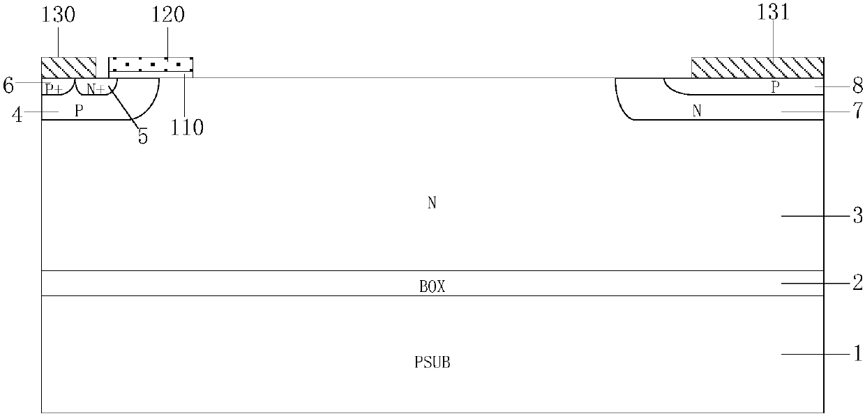
[0030] Such as image 3 As shown, the schematic diagram of the structure of this example includes a substrate 1, an insulating layer 2 and an N-type low-doped drift region 3 stacked from bottom to top; the upper layer of the N-type low-doped drift region 3 has two sides respectively P-type body region 4 and N-type buffer region 7, the upper layer of said P-type body region 4 has P+ contact region 6 and N+ emitter region 5 arranged side by side, wherein N+ emitter region 5 is located on the side close to N-type buffer region 7 The N-type buffer area 7 has a P-type collector region 8; the upper surface of the P+ contact region 6 and part of the N+ emitter region 5 has an emitter metal electrode 130, and the upper surface of the P-type body region 4 has a first A gate structure, the first gate structure is composed of a first gate dielectric layer 110 and a first polysilicon gate electrode 120 located on the upper surface of the first gate dielectric layer 110, and the lower surfac...

Embodiment 2

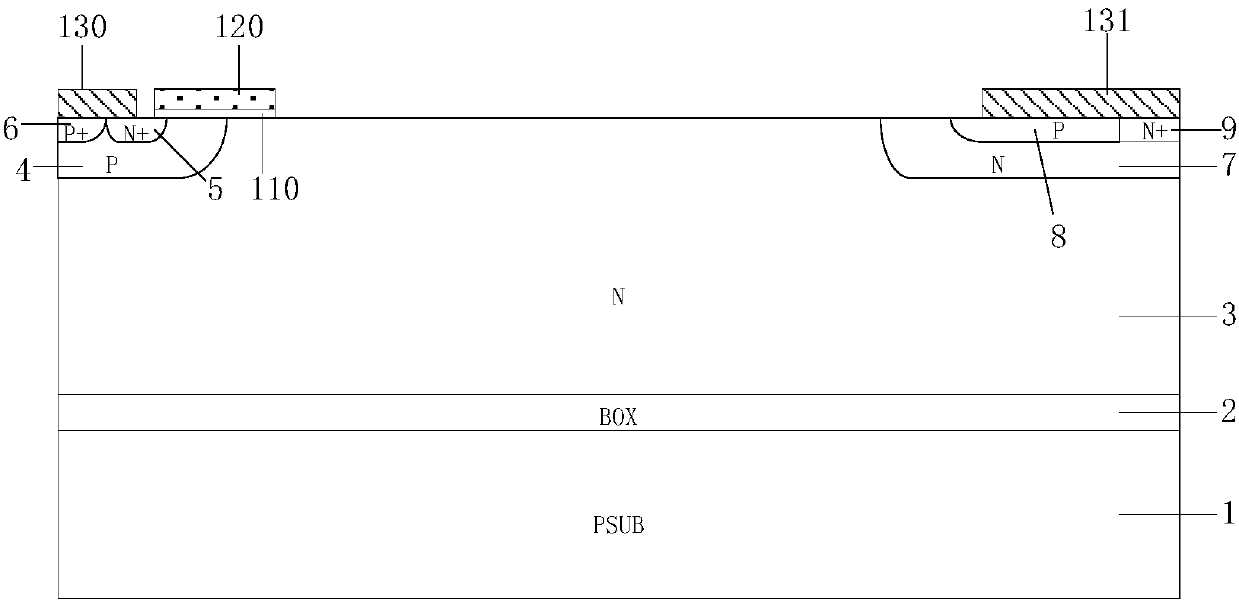
[0037] Such as Figure 4 As shown, the difference between this embodiment and Embodiment 1 is that compared with Embodiment 1, in this embodiment, the P-type collector region 8 and the collector metal electrode 131 and the highly doped N+ region 9, the highly doped P+ region 10 and The position of the third metal electrode 134 is interchanged. Therefore, in this example, the P-type collector region 8 is closer to the P-type body region 4 than the N+ region 9 and P+ region 10; compared with Example 1, the P-type collector region 8 and the N-type low-doped drift region are reduced. The thickness of the equivalent N-type buffer layer 7 between 3 and 3 further reduces the conduction loss of the device.

Embodiment 3

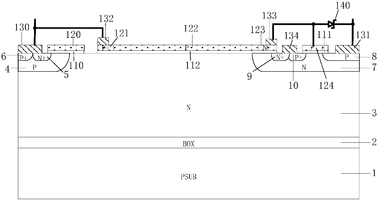
[0039] Such as Figure 5 As shown, in this embodiment, compared with Embodiment 2, a Zener diode is directly formed in the polysilicon layer above the dielectric layer 112. The Zener diode and the polysilicon diode share a highly doped N+ region 123, and the highly doped N+ region 123 is The anode of the Zener diode, the polysilicon N+ region 126 is the cathode of the Zener diode, and the polysilicon P+ region 125 is the highly doped region between the anode and cathode of the Zener diode; meanwhile, the Zener diode type in the polysilicon layer above the dielectric layer 112 , The position and shape can be adjusted as required, for example, the N + region 126 and P + region 125 can be arranged in the width direction of the device perpendicular to the horizontal direction; compared with embodiment 2, the integration is improved and the chip area is reduced.


PUM


Abstract

The invention belongs to the semiconductor power device technology field, and particularly relates to a transverse insulated gate bipolar transistor. In the invention, a poly-diode is formed on a surface of a drift region of a member and a PMOS and a Zener diode are formed in proximity to a collector; in a blocking state, under an action of charges and a field plate which are supplied through depleting the drift area in a reverse bias state of a polycrystalline diode on the surface of the member, voltage resistance higher than that that of a traditional structure is obtained while a doping concentration of the drift region of the member; in a process of switching off the member, a voltage change of a collector and a self-bias effect formed by a surface polycrystalline diode and a zener diode make PMOS near the collector automatically start and conduct and accelerate carrier extraction in an LIGBT so as to improve switching off speed of the member; in a conductive state, the PMOS around the collector is in a switching off state and an access of electronic current is cut off. As a result, the transverse insulated gate bipolar transistor has higher breakthrough voltage, and, in the process of switching off, has faster switching off speed and switching off loss.

Description

Technical field [0001] The invention belongs to the technical field of semiconductor power devices, and specifically relates to a lateral insulated gate bipolar transistor. Background technique [0002] Insulated gate bipolar transistor (IGBT) is a new type of power electronic device that combines MOS field effect and bipolar transistor. It not only has the advantages of easy drive and simple control of MOSFET, but also has the advantages of reduced conduction voltage of power transistor, and the on-state With the advantages of large current and low loss, it has become the mainstream power switching device in the field of medium and high power power electronics, which is widely used in various fields of the national economy such as communications, energy, transportation, industry, medicine, household appliances, and aerospace. Internationally renowned semiconductor companies, such as ABB, Infineon (IR), ST, Renesas, Mitsubishi, FuJi, etc. have successively invested in the develop...

Claims


Application Information

Patent Timeline
Patent Type & Authority Applications(China)
IPC IPC(8): H01L29/739H01L27/06
CPCH01L27/0629H01L29/7394
Inventor 张金平陈钱刘竞秀李泽宏任敏张波
Owner UNIV OF ELECTRONICS SCI & TECH OF CHINA
Why Eureka
Try Eureka