Lateral insulated gate bipolar transistor

A technology of bipolar transistors and insulated gates, applied in the direction of electric solid-state devices, semiconductor devices, electrical components, etc., can solve the problems of weakening the conductance modulation effect in the drift region, unfavorable practical application of devices, and increasing the forward conduction voltage drop. The effect of high breakdown voltage, low turn-off loss, and fast turn-off speed

Active Publication Date: 2017-09-15
UNIV OF ELECTRONIC SCI & TECH OF CHINA
View PDF4 Cites 12 Cited by
  • Summary
  • Abstract
  • Description
  • Claims
  • Application Information

AI Technical Summary

Problems solved by technology

However, when the structure is in forward conduction, electrons reach the collector through the N+ emitter region 5, the surface channel of the P-type body region 4, the low-doped N-type drift region 3, and the collector N+ region 8, forming a parasitic MOS structure. The generatio

Method used


Image

  • Lateral insulated gate bipolar transistor
  • Lateral insulated gate bipolar transistor
  • Lateral insulated gate bipolar transistor

Examples


Embodiment 1

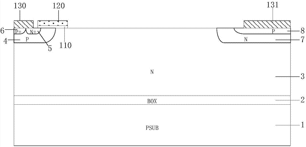
[0025] Such as image 3 As shown, it is a schematic structural diagram of this example, including a substrate 1, an insulating layer 2, and an N-type low-doped drift region 3 that are stacked sequentially from bottom to top; the upper sides of the N-type low-doped drift region 3 have respectively The P-type body region 4 and the N-type buffer zone 7, the upper layer of the P-type body region 4 has a P+ contact region 6 and an N+ emitter region 5 arranged side by side, wherein the N+ emitter region 5 is located on the side close to the N-type buffer region 7 , the N-type buffer area 7 has a P-type collector region 8 and a highly doped N+ region 9 arranged side by side, wherein the P-type collector region 8 is located on the side close to the P-type body region 4; the P+ contact The upper surface of the region 6 and part of the N+ emitter region 5 has an emitter metal electrode 130, and the upper surface of the P-type body region 4 has a first gate structure, and the first gate ...

Embodiment 2

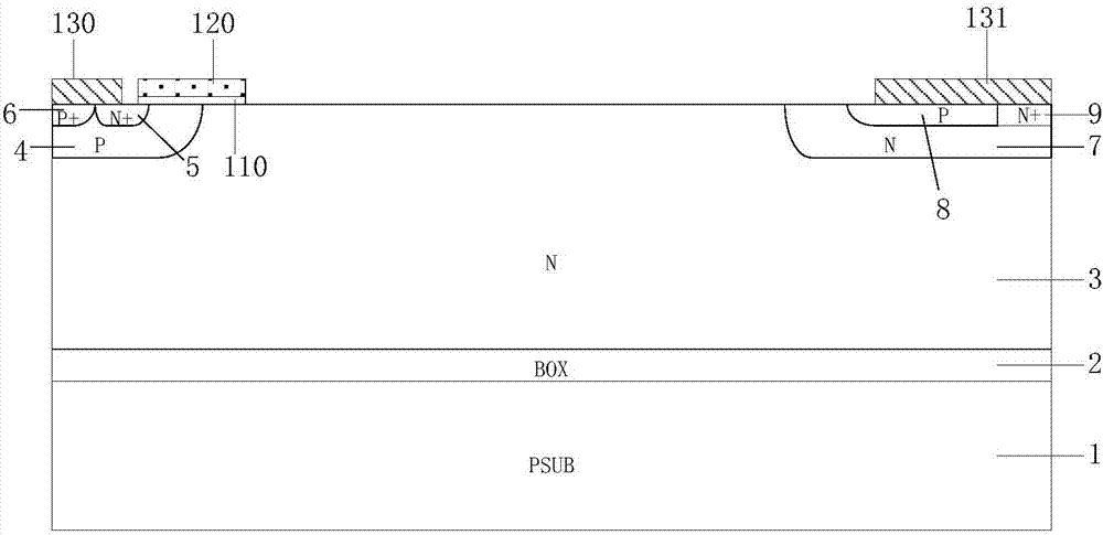
[0032] Such as Figure 4 As shown, the difference between this example and Example 1 is that in this example, compared with Example 1, the N+ region 10, the second P-type region 12, the dielectric layer 111, the polysilicon electrode 121, and the N-type low-doped drift region 3 and the PMOS formed by the first P-type region 11 is formed in the N-type well region 13 located on the surface of the N-type low-doped drift region 3 , the concentration of the N-type well region 13 is greater than the concentration of the N-type low-doped drift region 3 . Therefore, the breakdown voltage of the PMOS device in this example can be further increased, further improving the breakdown voltage of the device.

Embodiment 3

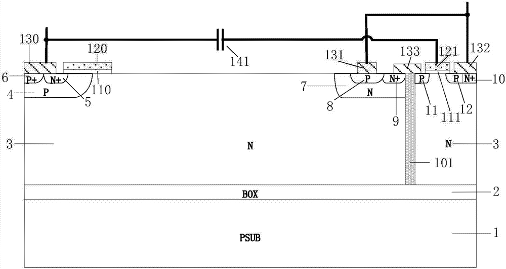
[0034] Such as Figure 5 As shown, compared with Embodiment 2, this example has a Zener diode 151 between the first metal electrode 132 and the second polysilicon electrode 121, wherein the cathode of the Zener diode 151 is connected to the first metal electrode 132 and the second polysilicon electrode 121. The collector metal electrode 131, the anode of the Zener diode 151 is connected to the second polysilicon electrode 121 and the capacitor 141; the stable voltage value of the Zener diode 151 is greater than the absolute value of the threshold voltage of the PMOS, and is less than that of the dielectric layer 111 of the PMOS device. Breakdown voltage value; the Zener diode 151 is integrated on the surface of the same device through a polysilicon layer. The Zener diode 151 further improves the charging and discharging speed of the capacitor 141, increases the turn-off speed of the LIGBT, reduces the turn-off loss, and improves the reliability of the integrated PMOS device. ...


PUM

PropertyMeasurementUnit
Thicknessaaaaaaaaaa
Thicknessaaaaaaaaaa
Thicknessaaaaaaaaaa

Abstract

The invention belongs to the technical field of a semiconductor power device, and specifically relates to a lateral insulated gate bipolar transistor. On the basis of a conventional positive electrode short circuit LIGBT structure, an isolation dielectric groove is formed in one end of a collector in a device drift region; an integrated PMOS structure is formed at the other end of the isolation dielectric groove, and the integrated PMOS structure is connected with a positive electrode short circuit N+ region in series; and meanwhile, an integrated capacitive structure is introduced between the gate of the integrated PMOS structure and the emitter of the LIGBT device. By virtue of a self-biasing effect formed by the integrated PMOS structure and the capacitor, the lateral insulated gate bipolar transistor has the same working condition as the conventional LIGBT and the same conduction voltage drop, without causing a negative impedance phenomenon in the conduction process, in the conduction state; in a blocking state, the lateral insulated gate bipolar transistor has higher breakdown voltage; and meanwhile, in the switching-off process, the lateral insulated gate bipolar transistor has higher switching-off speed and lower switching-off loss.

Description

technical field [0001] The invention belongs to the technical field of semiconductor power devices, and in particular relates to a lateral insulated gate bipolar transistor. Background technique [0002] Insulated gate bipolar transistor (IGBT) is a new type of power electronic device combined with MOS field effect and bipolar transistor. The advantages of large current and low loss have become the mainstream power switching devices in the field of medium and high power power electronics, and are widely used in various fields of the national economy such as communications, energy, transportation, industry, medicine, household appliances, and aerospace. Internationally well-known semiconductor companies, such as ABB, Infineon (IR), ST, Renesas, Mitsubishi, FuJi, etc. have successively invested in the R&D and manufacturing of IGBTs. In recent years, as a hot field of power electronics, IGBT has received great attention from developed countries and regions such as the United S...

Claims


Application Information

Patent Timeline
IPC IPC(8): H01L29/739H01L27/06
Inventor 张金平赵倩刘竞秀李泽宏任敏张波
Owner UNIV OF ELECTRONIC SCI & TECH OF CHINA
Why Eureka
Try Eureka