Construction method of nanowire and data storage method

A data storage and nanowire technology, applied in the fields of nanomagnetism, nanotechnology, nanotechnology, etc., can solve inconclusive problems, reduce the preparation cost, realize multi-state operation and multi-value storage, improve process stability and The effect of preparation efficiency

Inactive Publication Date: 2017-08-18
INST OF MICROELECTRONICS CHINESE ACAD OF SCI
View PDF1 Cites 0 Cited by
  • Summary
  • Abstract
  • Description
  • Claims
  • Application Information

AI Technical Summary

Problems solved by technology

[0003] Simultaneously realize the controllable modulation of resistance state and ferromagnetism in the same device to obtain new multi-functional memory devices, realize multi-state operation and multi-value storage of memory devices has been a current research hotspot, but how to realize it has not yet been determined.

Method used


Image

  • Construction method of nanowire and data storage method
  • Construction method of nanowire and data storage method
  • Construction method of nanowire and data storage method

Examples


Embodiment 1

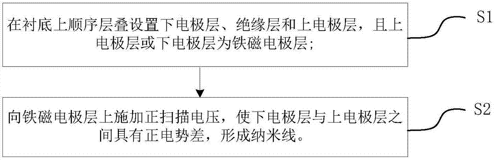
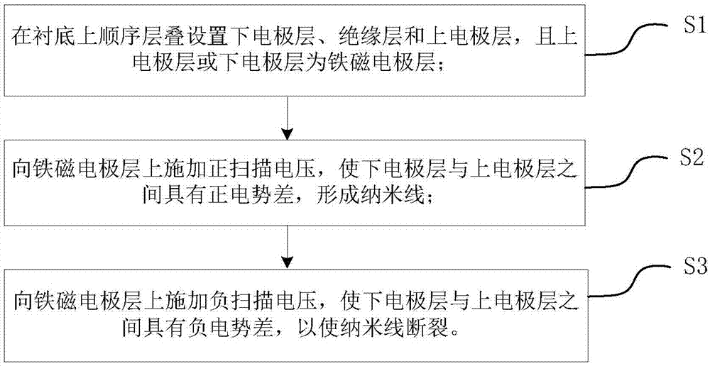
[0049] The method for constructing nanowires provided in this embodiment includes the following steps:

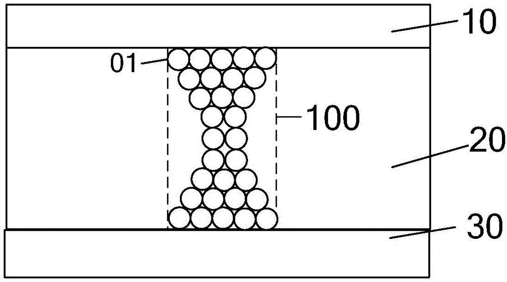
[0050] First, a seed layer, a lower electrode layer, an insulating layer, and an upper electrode layer are sequentially stacked on a substrate to form a resistive variable memory, wherein the substrate is SiO 2 substrate; the seed layer is a Ti metal film with a thickness of 10nm; then, the lower electrode layer is a Pt layer with a thickness of 30nm; the insulating layer is HfO with a thickness of 20nm 2 layer; the upper electrode layer is a 50nm Fe layer;

[0051] Then, the upper electrode layer is electrically connected with a semiconductor tester (Keithley 4200 / Agilent 1500), the lower electrode layer is grounded, and a positive voltage is applied to the upper electrode layer, and the resistance value of the memory is tested at the same time. The resistance value is increased by 10 5 ~10 7 Order of magnitude jump to 10 2 When the magnitude of , the applied positive s...


PUM

PropertyMeasurementUnit
thicknessaaaaaaaaaa
thicknessaaaaaaaaaa
thicknessaaaaaaaaaa

Abstract

The invention provides a construction method of a nanowire and a data storage method. The construction method of the nanowire comprises the following steps of S1, sequentially arranging a lower electrode layer, an insulation layer and an upper electrode layer on a substrate in a lamination way, wherein the upper electrode layer or the lower electrode layer is a ferromagnetic electrode layer; and S2, applying a positive scanning voltage onto the ferromagnetic electrode layer so that positive potential difference exists between the lower electrode layer and the upper electrode layer to form the nanowire. Compared with the construction method of the nanowire in the prior art, the construction method provided by the invention has the advantages that the preparation process is simplified, the preparation cost is reduced, the process stability and the preparation efficiency are improved, and the construction method can be widely applied and promoted; and moreover, after the construction method of the nanowire is applied to a storage structure of M/I/M, a resistance random access effect and a spin correlation effect can be simultaneously achieved, so that multi-state operation and multi-value storage in a simple structure are achieved, and a carrier is provided for a multi-stage storage device by a magnetoelectric coupling effect.

Description

technical field [0001] The invention relates to the technical field of nano devices and nano processing, in particular to a method for constructing nano wires and a data storage method. Background technique [0002] A wide variety of magnetic sensors based on the AMR effect have been widely used in the industry, especially in the field of information technology. In 1984, the AMR effect was used to realize high-density magnetic storage of information for the first time, which was of epoch-making significance at that time. In recent years, people have developed many new information materials and devices. Such as flash memory, resistive variable memory (RRAM), magnetic recording, etc. [0003] Simultaneously realize the controllable modulation of resistance state and ferromagnetism in the same device to obtain new multi-functional memory devices, realize multi-state operation and multi-value storage of memory devices has been a current research hotspot, but how to realize it h...

Claims


Application Information

Patent Timeline
Patent Type & Authority Applications(China)
IPC IPC(8): H01L43/08H01L43/12B82Y40/00B82Y25/00B82Y10/00
CPCB82Y10/00B82Y25/00B82Y40/00H10N50/01H10N50/10
Inventor 龙世兵李磊磊滕蛟刘琦吕杭炳刘明
Owner INST OF MICROELECTRONICS CHINESE ACAD OF SCI
Why Eureka
Try Eureka