Zero cross detection circuit for synchronous buck converter
A technology of zero-crossing detection circuit and synchronous step-down, which is applied in the direction of instruments, measuring devices, and measuring electrical variables, etc. It can solve the problems that the detection deviation cannot be accurately offset, and achieve the effects of easy implementation, simple circuit structure, and improved accuracy
- Summary
- Abstract
- Description
- Claims
- Application Information
AI Technical Summary
Problems solved by technology
Method used
Image


Examples
Embodiment 1
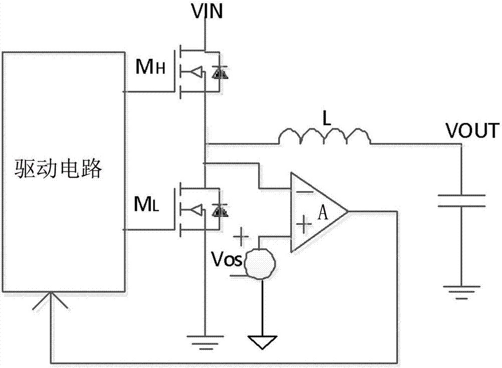
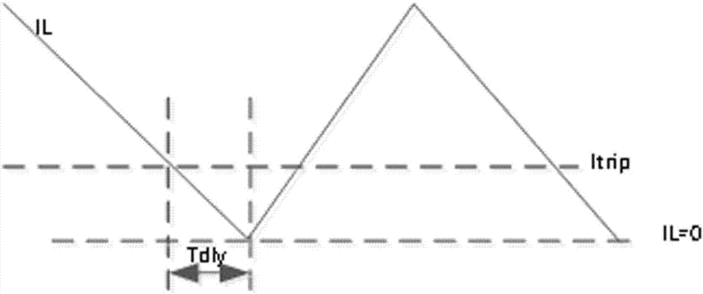
[0026] like image 3 As shown, a zero-crossing detection circuit for a synchronous step-down converter includes a zero-crossing comparator A and a multiplier, and the inverting input terminal of the zero-crossing comparator A is connected to the synchronous Tube M L The non-inverting input terminal of the zero-crossing comparator A is connected to the output terminal Vos of the multiplier, and the output terminal of the zero-crossing comparator A is connected to the input terminal of the driving circuit of the synchronous step-down converter, and the output terminal of the multiplier The first input terminal is connected to the voltage output terminal VOUT of the synchronous step-down converter, and the second input terminal of the multiplier is connected to a positive temperature coefficient current source Iptat.
[0027] In this specific embodiment, the multiplier includes PNP transistors M2-M5, NMOS transistors M0-M1 and resistors R0-R1, the emitter of the PNP transistor M...
Embodiment 2
[0032] The difference between this embodiment and Embodiment 1 is that the specific circuit structure of the multiplier is different, specifically, such as Figure 4 As shown, the multiplier includes NPN transistor M2, NPN transistor M3, PNP transistor M4, NPN transistor M5, NMOS transistor M0, PMOS transistor M1 and resistors R0-R1, the emitter of the NPN transistor M2 is grounded, and the NPN transistor M2 The collector of the triode M2 and the gate of the PMOS transistor M1 are connected to the output end of the first current mirror 1, the source series resistor R0 of the NMOS transistor M0 is grounded, and the gate of the NMOS transistor M0 is connected to the synchronous step-down converter. The voltage output terminal VOUT of the NMOS transistor M0 is connected to the input terminal of the first current mirror 1, the power supply terminal of the first current mirror 1 is connected to the power supply VCC, the base of the NPN transistor M2 and the emitter of the NPN tran...
PUM
 Abstract
Description
Claims
Application Information