Miniaturized CTS flat panel array antenna

An array antenna and flat panel technology, applied in antennas, antenna arrays, linear waveguide feed arrays, etc., can solve problems such as high assembly requirements, high processing requirements for offset parabolic reflectors, and large size.

Active Publication Date: 2017-09-05
NINGBO UNIV
View PDF4 Cites 20 Cited by
  • Summary
  • Abstract
  • Description
  • Claims
  • Application Information

AI Technical Summary

Problems solved by technology

[0004] However, the existing CTS flat-panel array antennas have the following problems: 1. The offset parabolic reflector of the flat-panel reflector requires a large space and a large size; 2. The processing requirements of the offset parabolic reflector are relatively high, and the , the focus of the offset parabolic reflector and the phase center of the H-plane fan-shaped horn antenna need to be strictly aligned, and the assembly requirements are high; 3. The waveguide power divider is formed by layering at least four waveguide power layers, and the size is large, and each Each waveguide power layer needs to be processed separately and then assembled. The assembly process is complicated and the assembly requirements are high.

Method used


Image

  • Miniaturized CTS flat panel array antenna
  • Miniaturized CTS flat panel array antenna
  • Miniaturized CTS flat panel array antenna

Examples


Embodiment 1

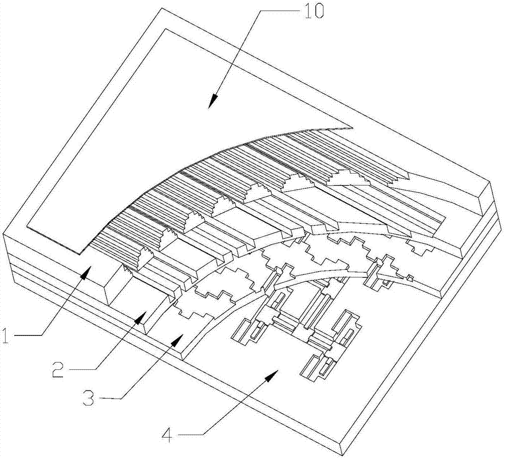
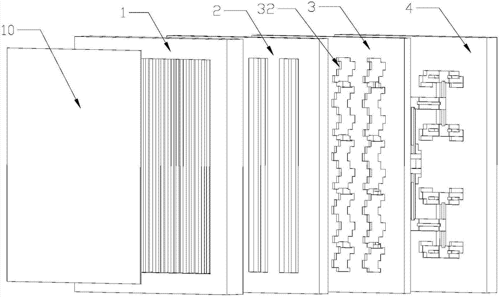
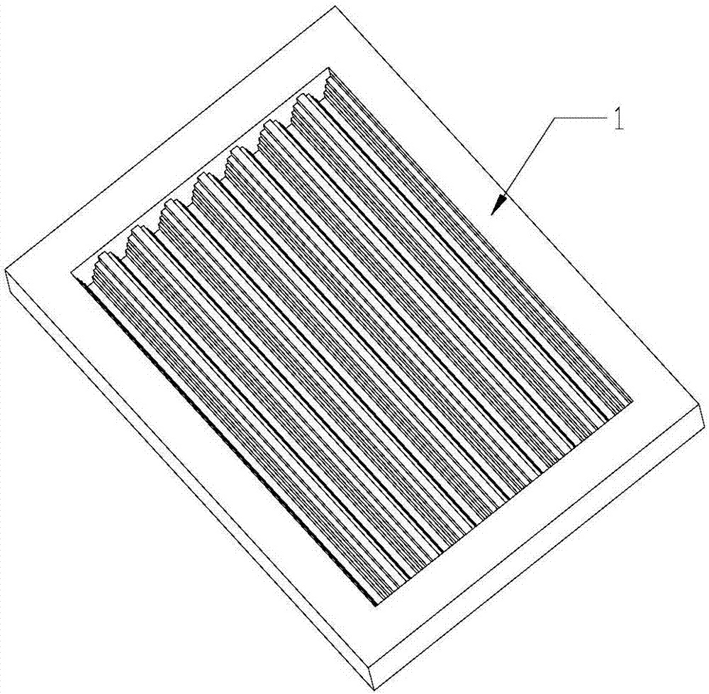
[0026] Embodiment one: if Figure 1-Figure 6 As shown, a miniaturized CTS panel array antenna includes a radiation layer 1, a waveguide work layer 2, a mode conversion layer 3 and a feed network layer 4 arranged in sequence from top to bottom; the mode conversion layer 3 includes a first metal plate 31 and the mode conversion cavity array 32 arranged on the upper surface of the first metal plate 31, the mode conversion cavity array 32 consists of n 2 The mode conversion cavities 33 are arranged in the form of n rows×n columns, n is an integer greater than or equal to 4, and the n mode conversion cavities 33 located in the same column are connected end to end in turn, and the mode conversion cavities 33 located in the kth row and the jth column The center distance between the mode conversion cavity 33 located in row k and column j+1 is between 1.5 times the wavelength and 2 times the wavelength, k=1, 2, 3, ..., n, j=1, 2 , 3, ..., n-1, the mode conversion cavity 33 includes a ...

Embodiment 2

[0029] Embodiment two: if Figure 1-Figure 6 As shown, a miniaturized CTS panel array antenna includes a radiation layer 1, a waveguide work layer 2, a mode conversion layer 3 and a feed network layer 4 arranged in sequence from top to bottom; the mode conversion layer 3 includes a first metal plate 31 and the mode conversion cavity array 32 arranged on the upper surface of the first metal plate 31, the mode conversion cavity array 32 consists of n 2 The mode conversion cavities 33 are arranged in the form of n rows×n columns, n is an integer greater than or equal to 4, and the n mode conversion cavities 33 located in the same column are connected end to end in turn, and the mode conversion cavities 33 located in the kth row and the jth column The center distance between the mode conversion cavity 33 located in row k and column j+1 is between 1.5 times the wavelength and 2 times the wavelength, k=1, 2, 3, ..., n, j=1, 2 , 3, ..., n-1, the mode conversion cavity 33 includes a ...


PUM


Abstract

The invention discloses a miniaturized CTS flat panel array antenna. The miniaturized CTS flat panel array antenna comprises a radiation layer, a waveguide power dividing layer, a mode conversion layer and a feed network layer which are sequentially arranged from top to bottom, and is characterized in that the mode conversion layer comprises a first metal flat panel and a mode conversion cavity array arranged at the upper surface of the first metal flat panel, the mode conversion cavity array is formed by arranging n<2> mode conversion cavities according to an n*n mode, the feed network layer comprises 4<n> H-type single ridge waveguide power dividing networks, two rectangular waveguide-single ridge waveguide converters and an E-plane waveguide power divider, wherein n is an integer which is greater than or equal to 1, each H-type single ridge waveguide power dividing network is provided with an input end and four output ends, and the rectangular waveguide-single ridge waveguide converter is provided with a rectangular waveguide input end and a single ridge waveguide output end. The miniaturized CTS flat panel array antenna is small in size and simple in processing and assembling process on the basis of having wide frequency band, high gain and high efficiency.

Description

technical field [0001] The invention relates to a CTS panel array antenna, in particular to a miniaturized CTS panel array antenna. Background technique [0002] In recent years, high-sensitivity, wide-band and low-profile high-performance panel antennas have been widely used in wireless communication, ultra-wideband communication, and satellite communication due to their characteristics of multi-band and low cost. At present, the common forms of panel antenna mainly include microstrip array antenna, waveguide slot array antenna and CTS (continuous transverse stub) panel array antenna. The microstrip array antenna has the characteristics of low profile, miniaturization, light weight, and easy processing. However, when the frequency increases or the size of the antenna array becomes larger, the insertion loss of the microstrip antenna increases due to conductor loss and dielectric loss, which cannot meet the requirements. high frequency and high efficiency applications. The...

Claims


Application Information

Patent Timeline
Patent Type & Authority Applications(China)
IPC IPC(8): H01Q21/00H01Q1/50H01Q15/24
CPCH01Q1/50H01Q15/24H01Q21/0006H01Q21/0037
Inventor 尤清春黄季甫尤阳秦丽婷
Owner NINGBO UNIV
Why Eureka
Try Eureka