OLED array substrate and preparation method therefor and OLED display apparatus
An array substrate and insulating layer technology, which is applied in the manufacture of semiconductor/solid-state devices, semiconductor devices, electrical components, etc., can solve the problems of incomplete gray-scale display, affecting the display effect of OLED displays, etc., so as to improve the display effect and enhance the display effect. , to avoid the effect of voltage changes
- Summary
- Abstract
- Description
- Claims
- Application Information
AI Technical Summary
Problems solved by technology
Method used
Image
Examples
Embodiment 1
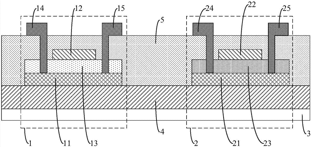
[0030] This embodiment provides an OLED array substrate, such as figure 1 As shown, it includes a switch tube 1 for controlling pixel display and a drive tube 2 for driving pixel display. The switch tube 1 includes a first insulating layer 13 disposed between its active layer 11 and gate 12; the drive tube 2 includes a second insulating layer 23 disposed between its active layer 21 and gate 22, and the dielectric constant of the first insulating layer 13 is higher than that of the second insulating layer 23.
[0031] By making the dielectric constant of the first insulating layer 13 higher than the dielectric constant of the second insulating layer 23, the capacitance between the grid 12 of the switching transistor 1 and the active layer 11 can be increased relative to the driving transistor 2, so that The subthreshold swing of the switch tube 1 is lower than that of the drive tube 2, thereby increasing the switching rate of the switch tube 1; at the same time, the capacitance...
Embodiment 2
[0046] This embodiment provides an OLED array substrate. The difference from Embodiment 1 is that the first insulating layer includes a bottom layer film and a top layer film overlapping each other, the bottom layer film is in contact with the active layer, and the top layer film is in contact with the gate. The bottom film is made of silicon dioxide, the top film is made of silicon nitride; the second insulating layer is made of silicon dioxide.
[0047] With such an arrangement, the bottom film of the silicon dioxide material is in contact with the active layer, which can reduce the interface defects of the active layer and improve the interface effect of the active layer, thereby making the switching control performance of the switching tube more stable.
[0048] Correspondingly, in this embodiment, the thickness of the bottom film is 30-50 nm, the thickness of the top film is 50-150 nm; the thickness of the second insulating layer is 120-200 nm.
[0049] The first insulati...
Embodiment 3
[0053] This embodiment provides an OLED display device, including the OLED array substrate in Embodiment 1 or 2.
[0054] By adopting the array substrate in embodiment 1 or 2, the response speed of the OLED display device is improved, and the display effect of the OLED display device is improved.
[0055] The OLED display device provided by the present invention can be any product or component with a display function such as an OLED panel, an OLED TV, a monitor, a mobile phone, a navigator, and the like.
PUM
| Property | Measurement | Unit |
|---|---|---|
| Thickness range | aaaaa | aaaaa |
| Thickness range | aaaaa | aaaaa |
| Thickness | aaaaa | aaaaa |
Abstract
Description
Claims
Application Information


