Semiconductor device with buffer layer and manufacturing method thereof

A manufacturing method and semiconductor technology, applied in the fields of semiconductor devices, semiconductor/solid-state device manufacturing, transistors, etc., can solve the problems of reducing the thermal budget, inability to achieve, and difficult to avoid high temperature annealing process, etc., to reduce the thermal budget, save equipment costs, The effect of reducing the turn-on voltage drop

Active Publication Date: 2018-05-01
ZHUZHOU CRRC TIMES SEMICON CO LTD
View PDF7 Cites 0 Cited by
  • Summary
  • Abstract
  • Description
  • Claims
  • Application Information

AI Technical Summary

Problems solved by technology

However, for field-stop IGBT devices, an N-type buffer layer is also required on the back side. If only P-type amorphous silicon is formed on the back side of DMOS, and the N-type buffer layer adopts traditional technology, it is difficult to avoid high-temperature annealing process, and it is impossible to reduce the thermal budget. Effect

Method used


Image

  • Semiconductor device with buffer layer and manufacturing method thereof
  • Semiconductor device with buffer layer and manufacturing method thereof
  • Semiconductor device with buffer layer and manufacturing method thereof

Examples


Embodiment Construction

[0041] For the sake of reference and clarity, the technical terms, abbreviations or abbreviations used below are recorded as follows:

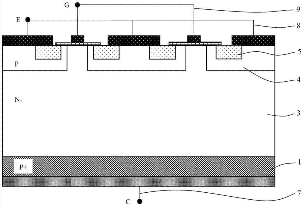
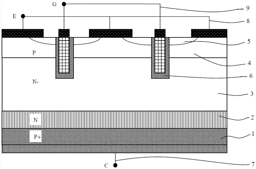
[0042] IGBT: Insulated Gate Bipolar Transistor, short for insulated gate bipolar transistor;

[0043] NPT: Non-Punch Through, the abbreviation of non-punch through;

[0044] E: Emitter, the abbreviation of emitter;

[0045] G: Gate, the abbreviation of gate;

[0046] C: Collector, short for collector;

[0047] MOS: Metal Oxid Semiconductor, the abbreviation of Metal Oxide Semiconductor;

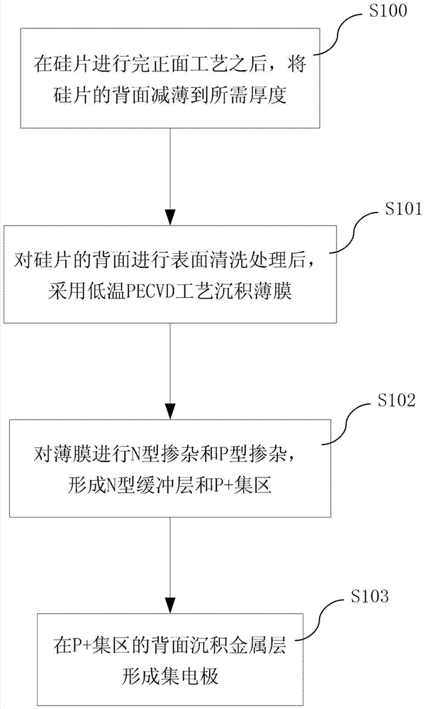
[0048] PECVD: Plasma Enhanced Chemical Vapor Deposition, the abbreviation of plasma enhanced chemical vapor deposition;

[0049] DMOS: double-diffused MOSFET, the abbreviation of double-diffused metal oxide semiconductor field effect transistor.

[0050]In order to make the purpose, technical solutions and advantages of the embodiments of the present invention more clear, the technical solutions in the embodiments of the present invention will be clearly...


PUM


Abstract

The invention discloses a semiconductor device having a buffer layer and a manufacturing method thereof. The semiconductor device comprises a front surface structure arranged on the front surface of the semiconductor device and a back surface structure arranged on the back surface of the semiconductor device. The back surface structure comprises a P<+> collector region and the N-type buffer layer arranged on the P<+> collector region. The P<+> collector region and the N-type buffer layer each adopt a thin film structure which is formed directly on the back surface of the semiconductor device by utilizing the low-temperature PECVD technology. The P<+> collector region and the N-type buffer layer further adopt the deposited thin film structure formed through the low temperature PECVD technology. The thin film is one or more of amorphous silicon, microcrystalline silicon, carbon-doped amorphous silicon or silicon germanium. According to the semiconductor device having the buffer layer and the manufacturing method thereof, cost of the semiconductor device and thermal budget of the silicon wafer back surface technology can be reduced effectively on the basis of not using an ion implantation device and an annealing process, and injection and extraction rate of carriers on the back surface of a silicon wafer can be adjusted according to the difference of the types of thin-film materials.

Description

technical field [0001] The invention relates to the field of semiconductor devices, in particular to a semiconductor device with a buffer layer structure and a manufacturing method thereof. Background technique [0002] With the rapid development of power electronics and semiconductor technology, various power electronics applications require the use of specialized and professional semiconductor switching devices to achieve a balance between cost and performance. as attached figure 1 Shown is a schematic structural diagram of a field stop type IGBT device in the prior art. The field stop type IGBT device includes a P+ collector region 1, an N-substrate 3, a P-type base region 4, an N+ emitter region 5, a collector electrode 7, and an emitter electrode 8 and grid 9. Compared with traditional non-punch-through (NPT) IGBT devices, field stop IGBT further reduces saturation voltage drop and switching loss, which makes field stop IGBT devices very suitable for various soft swit...

Claims


Application Information

Patent Timeline
Patent Type & Authority Patents(China)
IPC IPC(8): H01L29/739H01L29/06H01L21/331H01L21/205
CPCH01L21/0262H01L29/0684H01L29/66333H01L29/7398
Inventor 肖海波苗笑宇刘根罗海辉黄建伟刘国友
Owner ZHUZHOU CRRC TIMES SEMICON CO LTD
Why Eureka
Try Eureka