Preparation method for Micro LED display device
A display device, one-to-one correspondence technology, applied in the direction of electric solid device, semiconductor device, electrical components, etc., can solve the problems of poor uniformity of quantum dots, lower yield and display quality, large pixel size, etc., to improve the uniformity of light output. performance, avoid mutual influence, and reduce the cost of equipment
- Summary
- Abstract
- Description
- Claims
- Application Information
AI Technical Summary
Problems solved by technology
Method used
Image

Examples
Embodiment 1
[0040] The following steps are used to prepare the Micro LED display device:
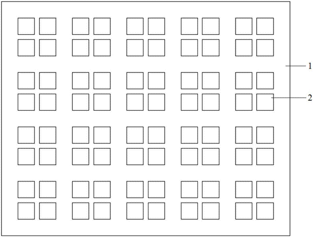
[0041] (1) Prepare an array of Micro LED chips 2 on the substrate 1, and the structure of the Micro LED chip array is as follows figure 1 shown;
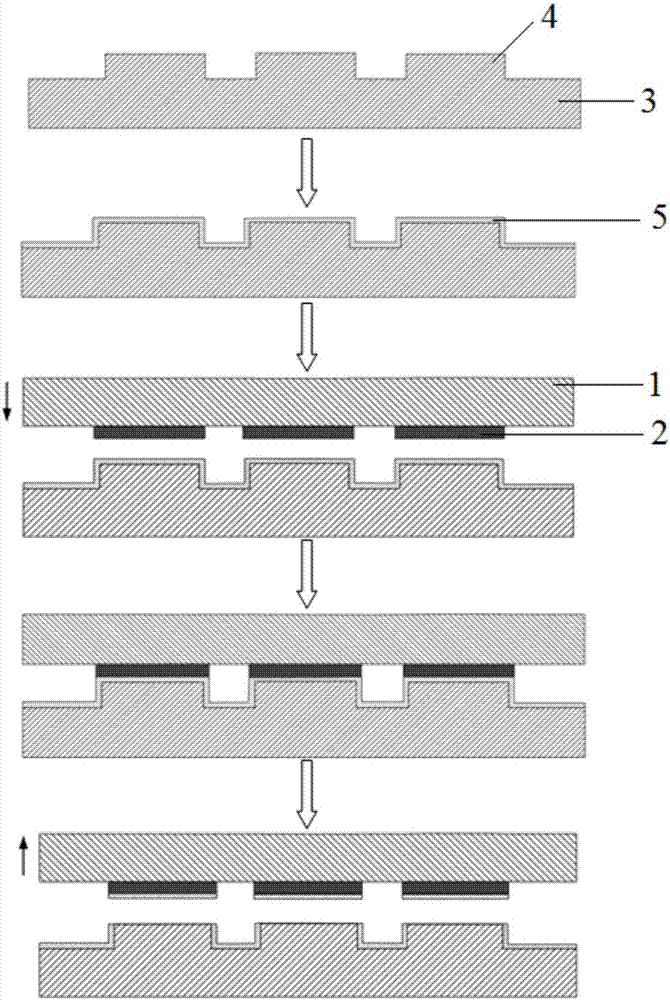
[0042] (2) according to figure 2 The schematic flow chart for preparing the red quantum dot material layer is shown, and a layer of red quantum dot material is prepared on the Micro LED chip 2 array. Technical preparation of transfer template one 3, the prepared transfer template one 3 has a Micro LED chip located in row 2i-1, column 2j-1 (i,j=1,2,3...n) of the Micro LED chip array 2 corresponds to the protrusion 4 pattern, the length of the protrusion 4 is 1.1 times the length of the chip 2, the width is 1.1 times the width of the chip 2, and the height is 2.1 times the height of the chip 2. The length and width of the protrusion are slightly larger than the length and width of the Micro LED chip, which can effectively reduce the blue light leakage o...
Embodiment 2
[0047] The following steps are used to prepare the Micro LED display device:
[0048] (1) Prepare a Micro LED chip 2 array on the substrate 1, the chip array is the same as in Example 1;
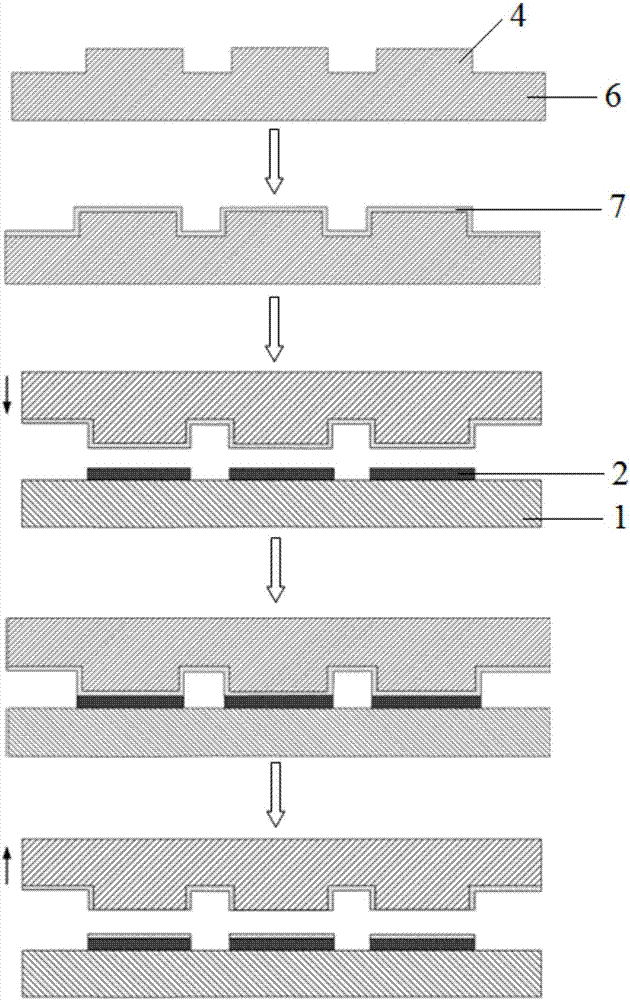
[0049] (2) according to Figure 6 The schematic flow chart for preparing the red quantum dot material layer is shown, and a layer of red quantum dot material is prepared on the Micro LED chip 2 array. Preparation of transfer template 3 8 by photolithography, the prepared transfer template 3 8 has an array of Micro LED chips 2 located at row 2i-1, column 2j-1 and row 2i, column 2j (i,j=1,2 , 3...n) Micro LED chip 2 corresponding to the bump 4 pattern, the length of the bump 4 is 1.3 times the length of the chip 2, the width is 1.1 times the width of the chip 2, and the height is 0.9 times the chip 2 The thickness of the transfer template has a raised pattern dipped in the quantum dot material 9, the quantum dot material is an aqueous solution of red quantum dots, the transfer template 3 8 i...
Embodiment 3
[0052] The following steps are used to prepare the Micro LED display device:
[0053] (1) Prepare a Micro LED chip 2 array on the substrate 1, the chip array is the same as in Example 1;
[0054] (2) according to Figure 8 The schematic flow chart for preparing the quantum dot material layer is shown, and a layer of quantum dot material is prepared on the Micro LED chip 2 array: Preparation of transfer template 5 12: Select PDMS as the transfer template material, and use nanoimprint technology to prepare the transfer template. Printing template 5 12, the prepared transfer printing template 5 12 has a pattern of depressions 13 corresponding to all the Micro LED chips 2 in the array of Micro LED chips 2, the length of the depression 13 is 1.1 times the length of the chip 2, and the width is 1.1 times the length of the chip 2 The width is 1 times the thickness of the chip 2 deep. The length and width of the depression are slightly larger than the length and width of the Micro L...
PUM
 Abstract
Description
Claims
Application Information
 - Generate Ideas
- Intellectual Property
- Life Sciences
- Materials
- Tech Scout
- Unparalleled Data Quality
- Higher Quality Content
- 60% Fewer Hallucinations
Browse by: Latest US Patents, China's latest patents, Technical Efficacy Thesaurus, Application Domain, Technology Topic, Popular Technical Reports.
© 2025 PatSnap. All rights reserved.Legal|Privacy policy|Modern Slavery Act Transparency Statement|Sitemap|About US| Contact US: help@patsnap.com