Three-dimensional packaging structure based on copper cylinders with different heights and manufacturing method thereof

A three-dimensional packaging, copper pillar technology, applied in the fields of semiconductor/solid-state device manufacturing, electrical components, electrical solid-state devices, etc., can solve the problems of high production cost, great difficulty, inability to realize signal delay of small package size of chips, etc., and achieve significant cost Advantages, the effect of reducing signal delay

Inactive Publication Date: 2017-09-22
NAT CENT FOR ADVANCED PACKAGING
View PDF3 Cites 1 Cited by
  • Summary
  • Abstract
  • Description
  • Claims
  • Application Information

AI Technical Summary

Problems solved by technology

These difficulties and costs are relatively easy to overcome for front-end wafer manufacturing plants or bumping (Bumping) production lines, but for wafer packaging plants, the production costs are too high and the difficulty is too great
[0005] Because the conventional wire-bonding packaging form of the packaging factory cannot meet the packaging requirements of small chip package size and low signal delay, at the same time, in view of the three-dimensional packaging form of the interposer board with through-silicon vias, the cost is too high and the difficulty is too great for the packaging factory , so a new packaging structure based on the existing equipment and technology of the packaging factory is needed to overcome the above problems

Method used


Image

  • Three-dimensional packaging structure based on copper cylinders with different heights and manufacturing method thereof
  • Three-dimensional packaging structure based on copper cylinders with different heights and manufacturing method thereof
  • Three-dimensional packaging structure based on copper cylinders with different heights and manufacturing method thereof

Examples


Embodiment Construction

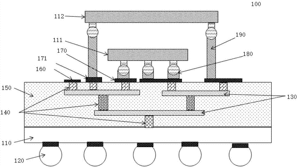
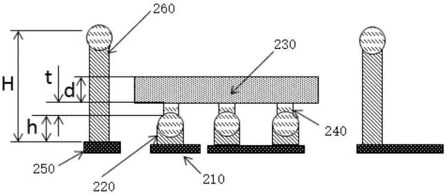
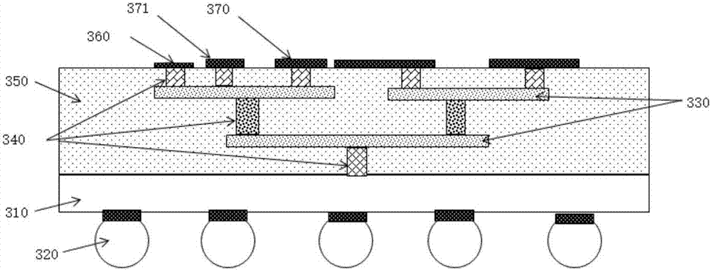
[0023] In the following description, the present invention is described with reference to various examples. However, one skilled in the art will recognize that the various embodiments may be practiced without one or more of the specific details, or with other alternative and / or additional methods, materials, or components. In other instances, well-known structures, materials, or operations are not shown or described in detail so as not to obscure aspects of the various embodiments of the invention. Similarly, for purposes of explanation, specific quantities, materials and configurations are set forth in order to provide a thorough understanding of embodiments of the invention. However, the invention may be practiced without these specific details. Furthermore, it should be understood that the various embodiments shown in the drawings are illustrative representations and are not necessarily drawn to scale.

[0024] In this specification, reference to "one embodiment" or "the ...


PUM


Abstract

The invention discloses a three-dimensional packaging structure based on copper cylinders with different heights. The three-dimensional packaging structure comprises a packaging substrate, an externally-connected welded ball positioned on the first surface of the packaging substrate, at least two layers of circuits positioned inside the packaging substrate and/or on the surface of the packaging structure, at least one layer of layer through holes, a first bonding pad and a second bonding pad which are positioned on the second surface of the packaging substrate, a first chip and a second chip which are positioned on the second surface of the packaging substrate, first copper pillar bumps positioned on the first chip and second copper pillar bumps positioned on the second chip, wherein the first chip is connected to the first bonding pad of the packaging substrate through the first copper pillar bumps; the second chip is connected to the second bonding pad of the packaging substrate through the second copper pillar bumps; the second copper pillar bump is higher than the first copper pillar bump; the first chip is at least partially positioned between the solder side of the second chip and the packaging substrate, so that the three-dimensional packaging structure is formed on the packaging substrate by the first chip and the second chip.

Description

technical field [0001] The invention relates to the field of semiconductor packaging, in particular to a three-dimensional packaging structure of a PCB substrate and a manufacturing method thereof. Background technique [0002] With the development of integrated circuit technology, in addition to the high-speed, low power consumption, and high reliability performance requirements for the device itself, in order to further meet the development of electronic products in the direction of miniaturization, intelligence, and integration, for Chip packaging poses higher challenges. Traditional packaging can no longer meet the requirements of high-performance chip packaging in many aspects such as package size and signal impedance. [0003] In traditional packaging, the interconnection of the package is generally realized by PCB board wiring bonding and wire bonding between chips. The length of the lead wire combined with the long wiring of the PCB board results in a large impedanc...

Claims


Application Information

Patent Timeline
Patent Type & Authority Applications(China)
IPC IPC(8): H01L23/498H01L23/488H01L21/60H01L25/065
CPCH01L23/49816H01L23/49827H01L24/16H01L24/81H01L25/0652H01L2224/16057H01L2224/16227H01L2224/8121H01L2224/81192H01L2924/15192H01L2924/15311H01L2224/16238
Inventor 李恒甫
Owner NAT CENT FOR ADVANCED PACKAGING
Why Eureka
Try Eureka