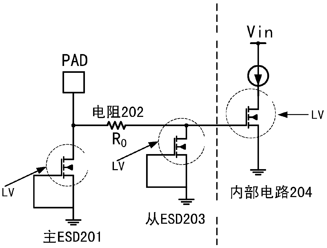
An electrostatic discharge esd protection circuit applied to integrated circuits
An ESD protection and integrated circuit technology, applied in emergency protection circuit devices, emergency protection circuit devices, circuits, etc. for limiting overcurrent/overvoltage, can solve electrical breakdown, oxide film rupture, metal wire melting, etc. problem, achieve the effect of reducing system power consumption and small leakage current
- Summary
- Abstract
- Description
- Claims
- Application Information
AI Technical Summary
Problems solved by technology
Method used
Image

Examples
Embodiment Construction
[0028] In order to make the object, technical solution and advantages of the present invention clearer, the present invention will be further described in detail below in conjunction with the accompanying drawings. Obviously, the described embodiments are only some embodiments of the present invention, rather than all embodiments . Based on the embodiments of the present invention, all other embodiments obtained by persons of ordinary skill in the art without making creative efforts belong to the protection scope of the present invention.
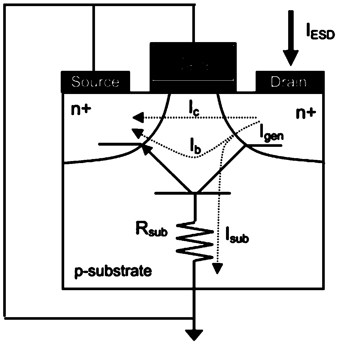
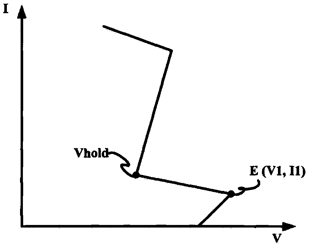
[0029] With the development of IC (Integrated Circuit, integrated circuit) design and manufacturing technology, the impact of ESD on integrated circuits is also increasing. Commonly used ESD protection devices include resistors, diodes, bipolar transistors, MOS transistors, SCR (Silicon Controlled Rectifier, silicon controlled thyristor) and the like. Due to the good compatibility between the MOS tube and the CMOS process, the MOS tube is ...
PUM
 Abstract
Description
Claims
Application Information