Manufacturing method of flash memory

A manufacturing method and memory technology, which are applied to semiconductor devices, electric solid-state devices, electrical components, etc., can solve the problem of poor step coverage of sidewall materials, decreased ability of the second sidewall 17 to isolate the floating gate FG and source lines, and rapid weakening. Flash and other problems, to achieve the effect of enhancing the density and improving the data retention ability

Active Publication Date: 2019-11-26
SHANGHAI HUAHONG GRACE SEMICON MFG CORP
View PDF2 Cites 0 Cited by
  • Summary
  • Abstract
  • Description
  • Claims
  • Application Information

AI Technical Summary

Problems solved by technology

[0010] It needs to be explained here that in the manufacturing process flow of the above-mentioned flash memory, after the FGSP1 DEP process is completed, the thickness of the oxide spacer material deposited at the bottom of the opening is usually thicker than that of the oxide spacer material deposited on the surface of the interlayer dielectric layer 14. The thickness of the side wall material is much thinner (approx. ), and when the FGSP1etch process is performed to form the sidewall 15, the shallow trench isolation structure 11 at the bottom of the opening will be lost, and when the FGSP1etch process is completed, the shallow trench isolation structure 11 will be lost by about Thus it is likely to expose the top corners of the active region 101 around it, such as Figure 1B As shown by the dotted line box 101 of , the exposed top corner of the active region 101 will be etched in the subsequent FGPL1 etch process and part of it will be lost, thereby forming Figure 1C The corner damage of the active area, that is, the active area recess (ACT recess or ACT Pits) 102, the active area recess 102 may lead to poor step coverage of the side wall material deposited in the FGSP2 DEP process, thereby causing the second side wall 17 The ability to isolate the floating gate FG and the source line is reduced, which weakens the data retention performance of the flash memory, and even causes the data retention failure issue of the flash memory; in addition, the chlorine concentration in the sidewall material deposited by the FGSP2 DEP process It may induce a leakage path between the source line polysilicon (SPL) and the floating gate FG filled in the opening subsequently, impairing the data retention performance of the flash memory

Method used


Image

  • Manufacturing method of flash memory
  • Manufacturing method of flash memory
  • Manufacturing method of flash memory

Examples


Embodiment Construction

[0044] In order to make the purpose and features of the present invention more obvious and understandable, the specific implementation of the present invention will be further described below in conjunction with the accompanying drawings. However, the present invention can be implemented in different forms and should not be limited to the described embodiments.

[0045] Please refer to figure 2 , the present invention proposes a kind of manufacturing method of flash memory, comprising:

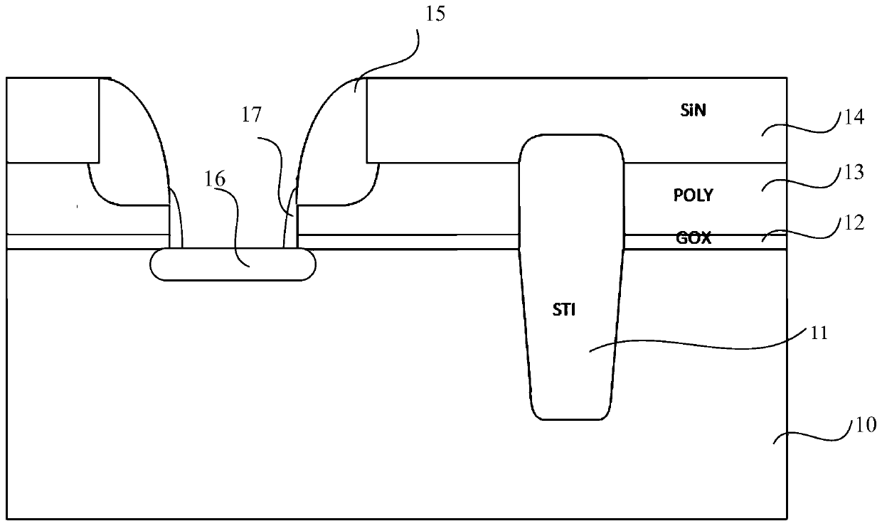
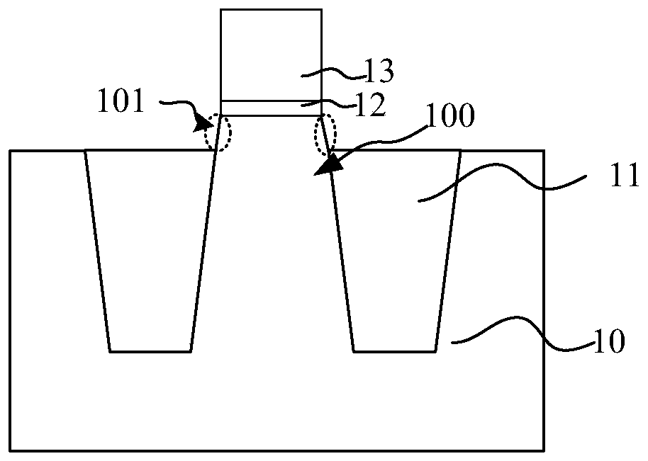
[0046] S1, providing a semiconductor substrate, sequentially forming a floating gate oxide layer, a floating gate layer, and an interlayer dielectric layer on the surface of the semiconductor substrate;

[0047] S2, etching the interlayer dielectric layer, and stopping to the surface of the floating gate layer, to form an opening;

[0048] S3, forming a first side wall on the side wall of the opening;

[0049] S4. Using the first sidewall as a mask, continue to etch the floating gate layer ...


PUM


Abstract

The invention provides a method for manufacturing a flash memory, after forming a source region or a drain region in the semiconductor substrate at the bottom of the opening after etching the floating gate layer and the floating gate oxide layer, and depositing the second side in the opening Before the wall material, a step is added to perform surface repair treatment on the floating gate exposed due to the depression of the active region at the junction of the active region and the shallow trench isolation region, so that the sidewall of the floating gate in the depression region of the open active region can be repaired damage, providing a good process surface for the material deposition of the second sidewall, which can solve the problem of poor isolation between the floating gate and the source line caused by the depression of the active area at the boundary of the shallow trench isolation structure, and improve the data retention capability of flash memory.

Description

technical field [0001] The invention relates to the field of semiconductor manufacturing, in particular to a method for manufacturing a flash memory. Background technique [0002] At present, flash memory (Flash memory), also known as flash memory, has become the mainstream of non-volatile memory. Its storage unit is based on the traditional MOS transistor structure, adding a floating gate (Floating Gate, FG) and a layer tunnel oxide (Tunnel Oxide), and use floating gates to store charges to achieve non-volatility of stored content, and shallow trench isolation (STI, Shallow Trench Isolation) structure is required for electrical isolation between memory cells . [0003] A typical manufacturing process of flash memory in the prior art includes FG OX / FG Poly / PAD SiN DEP→STI etch→STI Liner OX / STI HDP&CMP→ / PAD SiN remove→FG SiN DEP→FGPH / SiNetch→FGSP1 DEP / etch→FGPL1 etch→VSS IMP→FGSP2 DEP / etch, as follows: [0004] First, please refer to Figure 1A and Figure 1B , providing...

Claims


Application Information

Patent Timeline
Patent Type & Authority Patents(China)
IPC IPC(8): H01L27/11521
CPCH10B41/30
Inventor 徐涛李冰寒于涛
Owner SHANGHAI HUAHONG GRACE SEMICON MFG CORP
Why Eureka
Try Eureka