Power semiconductor chip, sub-module comprising the chip and crimping-type packaging module

A technology for power semiconductors and packaging modules, which is applied in the fields of semiconductor devices, semiconductor/solid-state device manufacturing, and semiconductor/solid-state device components, etc. The effect of improving pressure stability, improving yield and simplifying production process

Active Publication Date: 2017-10-10
ZHUZHOU CRRC TIMES SEMICON CO LTD
View PDF7 Cites 6 Cited by
  • Summary
  • Abstract
  • Description
  • Claims
  • Application Information

AI Technical Summary

Problems solved by technology

[0006] In view of this, the object of the present invention is to provide a power semiconductor chip, including a sub-module of the chip and a crimping package module, so as to solve the problem that the existing modules are difficult to achieve pressure balance between sub-modules and balanced contact of the interface. As well as the technical problems that the structure and process are complicated, the yield rate is difficult to improve, and it is difficult to achieve mass production

Method used


Image

  • Power semiconductor chip, sub-module comprising the chip and crimping-type packaging module
  • Power semiconductor chip, sub-module comprising the chip and crimping-type packaging module
  • Power semiconductor chip, sub-module comprising the chip and crimping-type packaging module

Examples


Embodiment 1

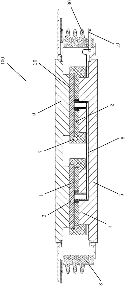
[0074] as attached figure 1 As shown, a specific embodiment of a crimping package module, the module 100 further includes:

[0075] Shell 30, the shell 30 comprises the shell 8 of ceramic material, the cap 9 as the first electrode, and the base 5 as the second electrode, the cap 9 is fixed on the top of the shell 8, the base 5 is fixed on the bottom of the shell 8 At the bottom, a grid terminal 10 as a third electrode is also provided on the shell 8;

[0076] More than two sub-modules 20 arranged in the housing 30, the sub-modules 20 realize parallel crimping through the tube cover 9 and the base 5; The grid electrodes are interconnected; one side of the sub-module 20 is connected to the tube cover 9, a part of the other side of the sub-module 20 is connected to the base 5, and the other part is connected to the PCB board 6, and is connected to the grid lead-out terminal 10 after being interconnected through the PCB. .

[0077] Wherein, the first electrode serves as the col...

Embodiment 2

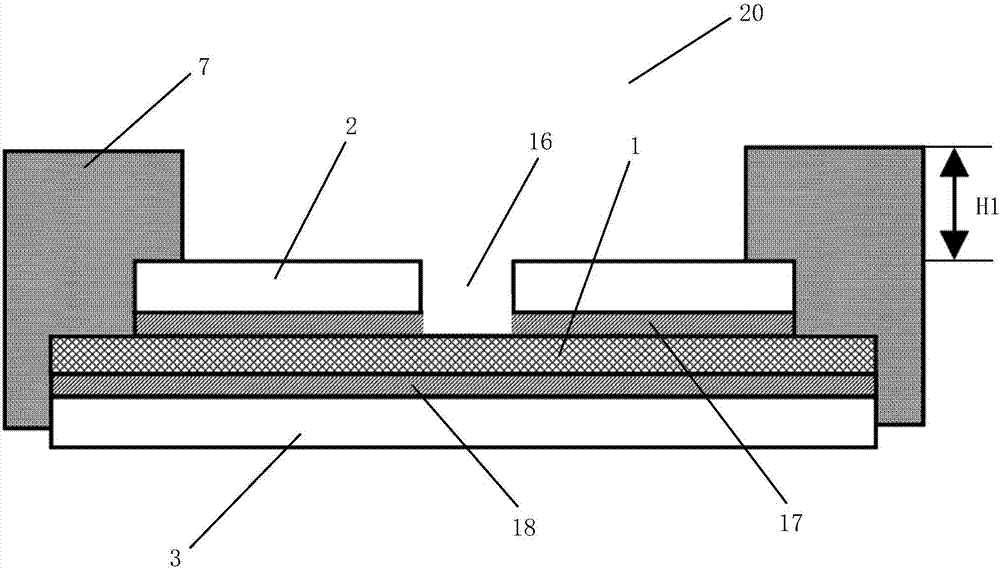
[0080] as attached figure 2 As shown, a specific embodiment of a sub-module 20 is shown. On the basis of Embodiment 1, the sub-module 20 further includes: an upper molybdenum sheet 2 , a lower molybdenum sheet 3 , and a chip 1 . The upper molybdenum sheet 2 is arranged on the upper surface of the chip 1 (between the chip 1 and the base 5 ), and the upper molybdenum sheet 2 is connected with the chip 1 through the upper sintering layer 17 . The lower molybdenum sheet 3 is arranged on the lower surface of the chip 1 (between the chip 1 and the cap 9 ), and the lower molybdenum sheet 3 is connected with the chip 1 through the lower sintering layer 18 . A through hole 16 for leading out the gate electrode 105 is provided at the center of the upper molybdenum sheet 2 . The upper molybdenum sheet 2 and the lower molybdenum sheet 3 are respectively connected to the upper and lower surfaces of the chip 1 through a silver sintered layer. The size of the molybdenum sheet is the same a...

Embodiment 3

[0085] as attached Figure 6 As shown, another specific embodiment of the sub-module 20 , on the basis of the first embodiment, the sub-module 20 further includes: an upper molybdenum sheet 2 , a lower molybdenum sheet 3 , and a chip 1 . The upper molybdenum sheet 2 is arranged on the upper surface of the chip 1 (between the chip 1 and the base 5 ), and the upper molybdenum sheet 2 is connected with the chip 1 through the upper sintering layer 17 . The lower molybdenum sheet 3 is arranged on the lower surface of the chip 1 (between the chip 1 and the cap 9 ), and the lower molybdenum sheet 3 is connected with the chip 1 through the lower sintering layer 18 . The periphery of the sub-module 20 is also provided with an insulating protective ring 7, the insulating protective ring 7 covers the terminal area 102 of the chip 1, the lower surface of the insulating protective ring 7 is higher than the lower surface of the lower molybdenum sheet 3, and the upper surface of the insulati...


PUM


Abstract

The invention discloses a power semiconductor chip, which includes a sub-module of the chip and a crimping package module. The chip includes: a terminal area, and an effective area located in the terminal area, and an emitter area and a gate are arranged in the effective area. Area. The gate region includes a gate electrode, a gate bus bar, and several peripheral gates located on the periphery of the gate electrode. The gate electrode is located in the center of the surrounding area of ​​the peripheral gate, and the gate electrode and the peripheral gate are connected through the gate bus bar. The area surrounded by the peripheral gate is divided into several sub-areas of the same size by the gate bus bar, and emitter electrodes are arranged in the sub-areas. Breakpoints are arranged between the peripheral gates, and the breakpoints are distributed centrally and / or axially symmetrically, and the emitter regions located in the surrounding area of ​​the peripheral gates and outside the peripheral gates are connected through the breakpoints. The invention can solve the technical problems that the existing modules are difficult to realize the balanced contact between the interfaces of the sub-modules, the structure and the process are complex, the yield rate is difficult to improve, and it is difficult to realize mass production.

Description

technical field [0001] The invention relates to the technical field of power electronics, in particular to a power semiconductor chip, including a sub-module of the chip and a crimping package module. Background technique [0002] With the development of technology and the continuous expansion of application fields, power semiconductor devices occupy an increasingly important position in modern power electronics technology. At present, power semiconductor devices are developing in the direction of high frequency, high power, intelligence and modularization. Among them, as a key technology for the application of power semiconductor devices, how to realize the high power capacity of power semiconductor modules has become the key direction of research and development in this technical field. In order to realize the high power capacity of the power semiconductor module, the prior art generally adopts a press-fit packaging technology in which dozens of chips are connected in par...

Claims


Application Information

Patent Timeline
Patent Type & Authority Applications(China)
IPC IPC(8): H01L21/68H01L23/16H01L25/07
CPCH01L25/072H01L21/68H01L23/16
Inventor 刘国友黄建伟窦泽春罗海辉覃荣震肖红秀张大华李继鲁肖强谭灿健戴小平
Owner ZHUZHOU CRRC TIMES SEMICON CO LTD
Why Eureka
Try Eureka