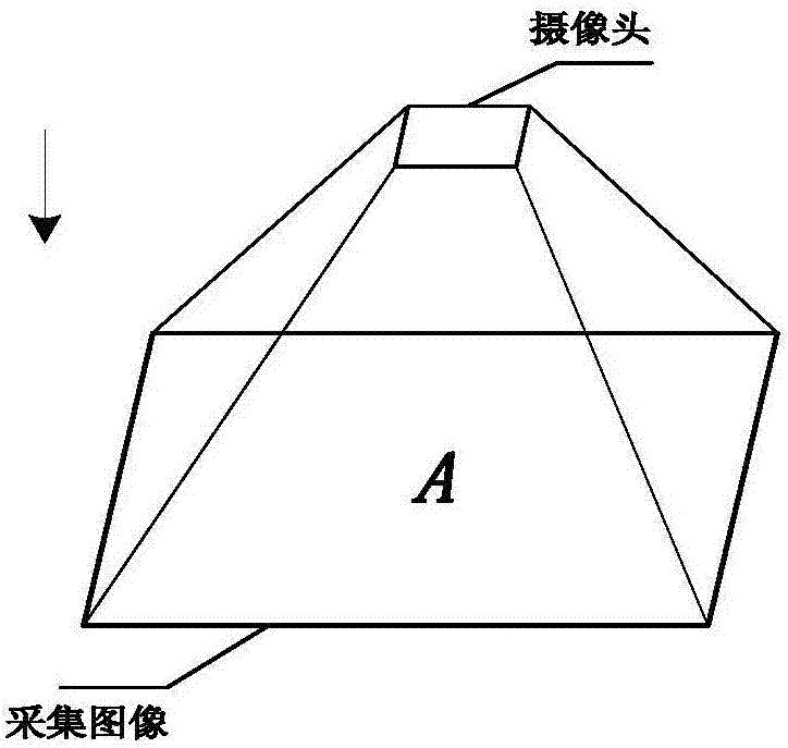
High-resolution image acquisition and processing device
A high-resolution image and processing device technology, applied in the field of high-resolution image acquisition and processing devices, can solve the problems of poor flexibility, poor applicability, and poor real-time processing ability, and achieve the effect of good flexibility
- Summary
- Abstract
- Description
- Claims
- Application Information
AI Technical Summary
Problems solved by technology
Method used
Image

Examples
Embodiment 1
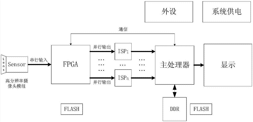
[0060] like Figure 4 As shown, it is a block diagram of FPGA internal functions. The main modules include lvds_video_rx module serial-to-parallel conversion module A, signal mapping rx_signal_mapping module B, cropping module C, and multi-channel synchronization module D.
[0061] The lvds_video_rx module A is mainly completed by the IP core provided by the FPGA supplier, such as the iddrx core of Lattice and the atllvds core of Altera. Since the differential data transmission paths of each channel are different (such as the length of PCB traces, etc.), transmission delays between channels will eventually occur. Therefore, the bit stream transmitted by each differential channel must be resolved separately according to the LVDS video transmission protocol. String, this module is to realize the deserialization of a single channel, output multiple channels of parallel data, and determine the data width such as 8bit or 10bit according to the configuration of the sensor.
[0062]...
Embodiment 2
[0113] Embodiment 2 is mainly aimed at the acquisition and preprocessing of ultra-high resolution images, and there is a discrepancy with Embodiment 1 mainly in the cropping unit and timing control unit.
[0114] For the acquisition and processing of ultra-high resolution images, due to its large data throughput, the required parallel pixel synchronization clock is also large. Therefore, for FPGAs that cannot support high read / write rate FIFOs internally, the principle of area speed exchange needs to be adopted.
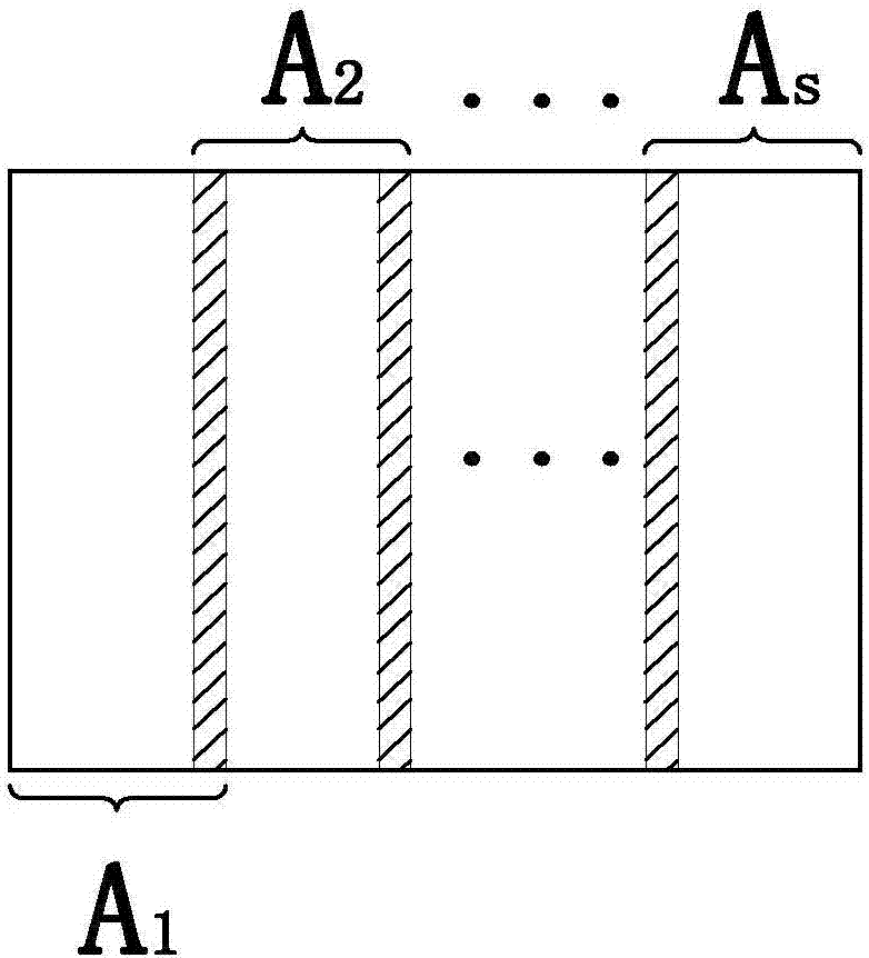
[0115] like Figure 11 As shown, the larger logic that was originally completed in one clock cycle is reasonably cut and completed in multiple clock cycles, and multiple times of logic resources are used to achieve the same function, thereby meeting the data throughput requirements. In this system, each asynchronous FIFO unit in the first embodiment needs to be replaced by y synchronous FIFOs, that is, s×y synchronous FIFOs are required to replace s asynchronous FIFO...
Embodiment 3
[0126] Embodiment 3 is similar to Embodiment 1, in that s asynchronous FIFOs are used to buffer data in different clock domains, and there is a discrepancy between the timing control unit and Embodiment 1 mainly. The first implementation mode is to perform write-while-read operations on s asynchronous FIFOs, and the third implementation mode adopts the mode of writing first and then reading.
[0127] The specific implementation process of embodiment 3 is as follows:
[0128] First, with w_clk (equal to f p ) Write the data of the first channel of the row that needs to be trimmed into the asynchronous FIFO. At this time, the read enable is set to invalid, and then the data of the second channel of the row is written in succession, ... until the sth channel of the row is written For the first data, the read operation is enabled for the s asynchronous FIFOs at the same time, and the image data of the s channels of the row is read out at the same time, so as to ensure the synchro...
PUM
 Abstract
Description
Claims
Application Information
 - R&D
- Intellectual Property
- Life Sciences
- Materials
- Tech Scout
- Unparalleled Data Quality
- Higher Quality Content
- 60% Fewer Hallucinations
Browse by: Latest US Patents, China's latest patents, Technical Efficacy Thesaurus, Application Domain, Technology Topic, Popular Technical Reports.
© 2025 PatSnap. All rights reserved.Legal|Privacy policy|Modern Slavery Act Transparency Statement|Sitemap|About US| Contact US: help@patsnap.com