
Printed circuit, thin film transistor and manufacturing method thereof

A technology for thin film transistors and printed circuits, applied to thin film transistors with operating voltages and their manufacturing fields, can solve problems such as reduced stability and shortened storage period, and achieve increased maintenance of electrical conductivity, increased heat resistance, improved stability and electrical conductivity. sexual effect

Active Publication Date: 2017-10-24
WINBOND ELECTRONICS CORP
View PDF10 Cites 0 Cited by
  • Summary
  • Abstract
  • Description
  • Claims
  • Application Information

AI Technical Summary

Problems solved by technology

Although the current conductive inks are mostly formed with highly stable gold and / or silver nanoparticles or nanowires, even so, when the conductive ink is exposed to the air, the stability will still be reduced and the shelf life will be shortened. question
In order to solve the above problems, most of the current solutions focus on the development of chemical synthesis methods, such as the formation of protective layers or protective films on metal nanoparticles, but such methods can only be used for specific metals.

Method used


Image

  • Printed circuit, thin film transistor and manufacturing method thereof
  • Printed circuit, thin film transistor and manufacturing method thereof
  • Printed circuit, thin film transistor and manufacturing method thereof

Examples


example 1

[0052] First, metallic ink containing silver nanowires is jet-printed on the substrate. Next, the metallic ink containing TiO 2 The colloidal composition of the precursor. Then, bake at 150 °C for 1 hour to remove the solvent and make the TiO 2 Precursors are reduced to TiO on the surface of silver nanowires 2 . So far, the substrate with TiO 2 Protective film for printed lines.

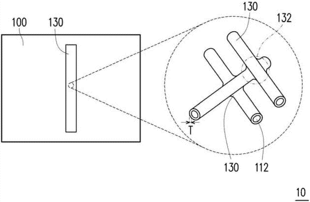
[0053] picture 5A It is a scanning electron micrograph of silver nanowires before printing the colloidal composition. picture 5B It is a scanning photo of the silver nanowires after spray printing the colloidal composition and baking. Depend on picture 5B It can be seen that after the spray-printed colloidal composition is baked, the colloid will not only form on the surface of the nano-silver wire, but also gather at the junction of the nano-silver wire, which contributes to the separation between adjacent nano-silver wires. bonding, thereby improving the stability and conductivity of...

example 2

[0055] Example 2 (jet printing metal ink and containing TiO 2 Colloidal composition of precursors)

[0056] First, metallic ink containing silver nanowires is jet-printed on the substrate. Next, the metallic ink containing TiO 2 The colloidal composition of the precursor. Then, a heating process is performed to remove the solvent. Next, after baking at 400° C. for 1 hour, the state of the silver nanowires was observed using a scanning electron microscope.

example 3

[0064] First, metallic ink containing silver nanowires is jet-printed on the substrate. Next, the metallic ink containing TiO 2 The colloidal composition of the precursor. Then, a heating process is performed to remove the solvent. Afterwards, after baking at 25°C, 50°C, 100°C, 150°C, 200°C, 250°C, 300°C, and 400°C for 1 hour, measure the sheet resistance of the silver nanowires with a protective film at each temperature point .


PUM

PropertyMeasurementUnit
widthaaaaaaaaaa
particle diameteraaaaaaaaaa

Abstract

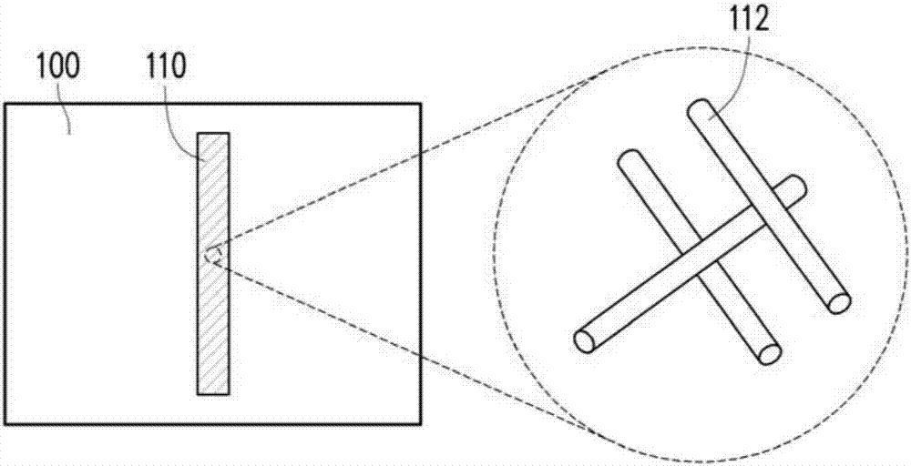
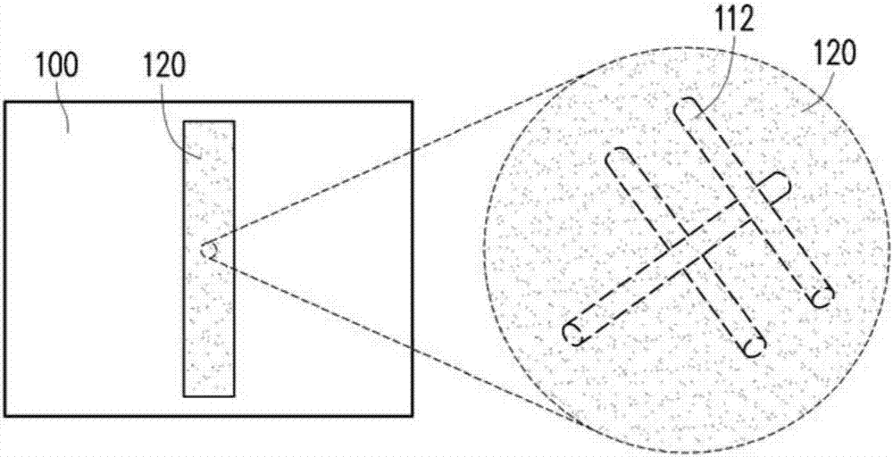
The invention provides a printed circuit, a thin film transistor and a manufacturing method thereof. The circuit structure comprises a plurality of metal nano-structures and a metal oxide layer, wherein the metal oxide layer is configured at the surfaces of the metal nano-structures and fills gaps at intersections of the metal nano-structures, and the thickness of the metal oxide layer configured at the surfaces of the metal nano-structures ranges between 0.1 nanometer and 10 nanometers. Meanwhile, the invention also provides a manufacturing method of the circuit, a thin film transistor and a manufacturing method thereof. The circuit structure can prevent entrance of moisture so as to avoid oxidation, can also increase the heat resistance and maintain the conductivity, and thus improves the stability and the conductivity of the circuit.

Description

technical field [0001] The present invention relates to a printed circuit, a thin film transistor and a manufacturing method thereof, in particular to a printed circuit with excellent heat resistance and conductivity, a thin film transistor with improved operating voltage and a manufacturing method thereof. Background technique [0002] In the current printed circuit manufacturing process, the conductive ink used is mostly made of nano-sized metal particles mixed with a solvent. However, since the metal particles are nanometerized, the oxidation rate of the formed metal structure will be greatly increased, thereby reducing its stability and shortening the storage period. Although the current conductive inks are mostly formed with highly stable gold and / or silver nanoparticles or nanowires, even so, when the conductive ink is exposed to the air, the stability will still be reduced and the shelf life will be shortened. question. In order to solve the above problems, most of ...

Claims


Application Information

Patent Timeline
Patent Type & Authority Applications(China)
IPC IPC(8): H01L29/786H01L29/06H01L23/485H01L21/60B81B1/00B81C1/00
CPCB81B1/00B81C1/00H01L21/02697H01L23/485H01L29/06H01L29/786H05K1/097H05K2203/1194H01L29/7869H01L21/02186H01L21/02288H05K2201/026H05K2201/0257H05K1/0201H05K1/09H05K1/0306H05K3/12H05K3/22H01L29/78618H01L29/45H01L21/288H01L29/66742H01L21/02175H05K2203/0783
Inventor 何羽轩
Owner WINBOND ELECTRONICS CORP
Learn More