Integrated packaging structure, and process for manufacturing integrated packaging structure

An integrated packaging and process technology, applied in the field of integrated packaging of optoelectronic devices, can solve the problems of degradation coefficient performance, loss fluctuation of pigtail fusion points, and easy polarization cross-coupling, etc., to eliminate differences in thermal expansion coefficients, reduce installation space requirements, and reduce deformation powerful effect

Active Publication Date: 2017-11-03
THE 44TH INST OF CHINA ELECTRONICS TECH GROUP CORP
View PDF4 Cites 4 Cited by
  • Summary
  • Abstract
  • Description
  • Claims
  • Application Information

AI Technical Summary

Problems solved by technology

[0003] The existing problem is: in the prior art, the semiconductor light-emitting device and the optical waveguide modulator in the optical transmitter are relatively independent, and the two are connected to each other by pigtail fusion. When applied, the length of the connecting fiber between the two Long, because the optical fiber cannot be bent with a small radius, the installation space takes up a lot; in addition, in harsh environments such as large temperature changes or strong vibration shocks, the loss of the pigtail splice point fluctuates greatly, and in severe cases, the splice point may even break In the case of opening, the entire system will fail to work; moreover, when the pigtail is a polarization-maintaining fiber, polarization cross-coupling is likely to occur at the fusion point, thereby introducing noise into the system and deteriorating the performance of the coefficient; overall, the existing The optical transmitter cannot meet the requirements of the system for performance, reliability and integration

Method used


Image

  • Integrated packaging structure, and process for manufacturing integrated packaging structure
  • Integrated packaging structure, and process for manufacturing integrated packaging structure

Examples


Embodiment Construction

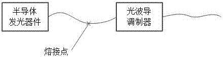
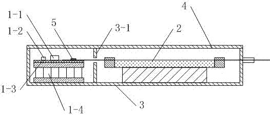
[0025] An integrated packaging structure, the structure of which is: the integrated packaging structure is composed of a semiconductor light emitting device, an optical waveguide modulator chip 2, a housing 3, a cover plate 4, a spacer 5, a connecting optical fiber, and an output pigtail;

[0026] The semiconductor light-emitting device is composed of a semiconductor light-emitting chip 1-1, a thermal diode 1-2, a heat sink 1-3 and a semiconductor refrigerator 1-4; the inner end of the connecting optical fiber and the input of the optical waveguide modulator chip 2 The inner end of the output pigtail is connected to the output end of the optical waveguide modulator chip 2; the housing 3 is provided with a mounting groove, and the middle part of the mounting groove is provided with a partition 3-1, and the partition 3 -1 divides the installation slot into slot A and slot B;

[0027] The semiconductor light emitting device is arranged in groove A; the bottom surface of the semic...


PUM


Abstract

The invention discloses an integrated packaging structure. The integrated packaging structure is composed of a semiconductor light-emitting device, an optical waveguide modulator chip, a shell, a cover plate, a limiting frame, a connecting optical fiber and an output tail fiber. The invention further discloses a process for manufacturing the integrated packaging structure. According to the invention, by adopting the integrated packaging structure and the process for manufacturing the integrated packaging structure, the size of a light emitting terminal machine can be effectively reduced. The requirement of the installation space is reduced, and the integration level of equipment is improved. Meanwhile, a series of problems caused due to the adoption of the welding connection mode are avoided.

Description

technical field [0001] The invention relates to a photoelectric device integrated packaging technology, in particular to an integrated packaging structure and a process for making the integrated packaging structure. Background technique [0002] In high-speed optical communication and microwave photonic signal transmission and processing systems, a typical optical transmitter is composed of a semiconductor light emitting device and an optical waveguide modulator. The connection method of the semiconductor light emitting device and the optical waveguide modulator is as follows: figure 1 As shown, the output pigtail of the semiconductor light-emitting device is fused with the input pigtail of the optical waveguide modulator to form an optical connection; the semiconductor light-emitting device mainly uses a high-power DFB semiconductor laser to provide the system with narrow linewidth, low noise, and high-power output The optical waveguide modulator uses electro-optic, thermo-...

Claims


Application Information

Patent Timeline
Patent Type & Authority Applications(China)
IPC IPC(8): G02B6/42H04B10/50
CPCG02B6/4237G02B6/4239G02B6/4244G02B6/4245G02B6/4296H04B10/501
Inventor 华勇田自君雷成龙郑帅峰
Owner THE 44TH INST OF CHINA ELECTRONICS TECH GROUP CORP
Why Eureka
Try Eureka