Pseudohalogen induction-based two-dimensional perovskite electric storage device and preparation method therefor

A pseudo-halogen and electric storage technology, which is applied in the field of two-dimensional perovskite 2PbI22 electric storage devices and its preparation, can solve the problems of complex preparation process and low ternary yield, and achieve simple preparation process and high ternary yield. Efficient, easy-to-operate effects

Active Publication Date: 2017-11-03
SUZHOU UNIV
View PDF4 Cites 5 Cited by
  • Summary
  • Abstract
  • Description
  • Claims
  • Application Information

AI Technical Summary

Problems solved by technology

[0003] Aiming at the problems of complex preparation process and low ternary yield of current organic electrical storage materials, the present invention discloses a pseudohalogen-induced two-dimensional perovskite (CH 3 NH 3 ) 2 PB 2 (SCN) 2 Electri...

Method used


Image

  • Pseudohalogen induction-based two-dimensional perovskite electric storage device and preparation method therefor
  • Pseudohalogen induction-based two-dimensional perovskite electric storage device and preparation method therefor
  • Pseudohalogen induction-based two-dimensional perovskite electric storage device and preparation method therefor

Examples


Embodiment 1

[0042] Under nitrogen protection, methyl ammonium iodide (635.8 mg, 4 mmol) was dissolved in DMF (2 mL), then lead thiocyanate (647.9 mg, 2 mmol) was added to the methyl ammonium iodide solution, shaken Obtain the yellow (CH 3NH 3 ) 2 PB 2 (SCN) 2 solution.

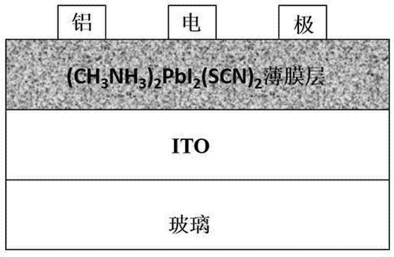
[0043] Pseudohalogen-induced two-dimensional perovskite electrical storage device structure such as figure 1 As shown, the device is basically divided into three layers, which are the ITO glass substrate layer, the active layer and the aluminum electrode layer from bottom to top. The preparation method, the specific steps are as follows:

[0044] 1. In an ultrasonic cleaner, clean the ITO glass substrate with deionized water, acetone, and absolute ethanol in sequence;

[0045] 2. The (CH 3 NH 3 ) 2 PB 2 (SCN) 2 The solution was spin-coated on an ITO glass substrate to form an active layer with a thickness of 250 nm, and then placed in a nitrogen-protected glove box to dry naturally to obtain a storage component...

Embodiment 2

[0050] Under nitrogen protection, methyl ammonium iodide (635.8 mg, 4 mmol) was dissolved in DMF (2 mL), then lead thiocyanate (647.9 mg, 2 mmol) was added to the methyl ammonium iodide solution, shaken Obtain the yellow (CH 3 NH 3 ) 2 PB 2 (SCN) 2 solution.

[0051] A method for preparing a pseudohalogen-induced two-dimensional perovskite electric storage device, the specific steps are as follows:

[0052] 1. In an ultrasonic cleaner, clean the ITO glass substrate with deionized water, acetone, and absolute ethanol in sequence;

[0053] 2. The (CH 3 NH 3 ) 2 PB 2 (SCN) 2 The solution was spin-coated on an ITO glass substrate to form an active layer with a thickness of 200 nm, and then placed in a nitrogen-protected glove box to dry naturally to obtain a storage component for a ternary electrical storage device; the spin-coating conditions were as follows: the solution was added dropwise to Immersion on the substrate for 60 s, the two speeds are: 1000 r / min for 25 s...

Embodiment 3

[0057] Under nitrogen protection, methyl ammonium iodide (635.8 mg, 4 mmol) was dissolved in DMF (2 mL), then lead thiocyanate (647.9 mg, 2 mmol) was added to the methyl ammonium iodide solution, shaken Obtain the yellow (CH 3 NH 3 ) 2 PB 2 (SCN) 2 solution.

[0058] A method for preparing a pseudohalogen-induced two-dimensional perovskite electric storage device, the specific steps are as follows:

[0059] 1. In an ultrasonic cleaner, clean the ITO glass substrate with deionized water, acetone, and absolute ethanol in sequence;

[0060] 2. The (CH 3 NH 3 ) 2 PB 2 (SCN) 2 The solution was spin-coated on an ITO glass substrate to form an active layer with a thickness of 300 nm, and then placed in a nitrogen-protected glove box to dry naturally to obtain a storage component for a ternary electrical storage device; the spin-coating conditions were as follows: the solution was added dropwise to Immersion on the substrate for 60 s, the two speeds are: 1000 r / min for 20 s...


PUM

PropertyMeasurementUnit
Thicknessaaaaaaaaaa
Thicknessaaaaaaaaaa
Thicknessaaaaaaaaaa

Abstract

The invention discloses a pseudohalogen induction-based two-dimensional perovskite (CH<3>NH<3>)<2>PbI<2>(SCN)<2> electric storage device and a preparation method therefor. The preparation method comprises the following steps of dissolving methyl amine iodide into a DMF solvent, and then adding lead thiocyanate into the solution, fully oscillating and preparing into a yellow perovskite solution; coating a substrate with the perovskite solution to prepare an active layer; and next, preparing an electrode on the active layer to obtain the pseudohalogen induction-based two-dimensional perovskite (CH<3>NH<3>)<2>PbI<2>(SCN)<2> electric storage device. The pseudohalogen induction-based two-dimensional perovskite material is formed by organic amine salt and the inorganic metallic compound through a coordination effect so as to prepare the organic electric storage device with the sandwich structure, so that an organic electric storage behavior is realized successfully; meanwhile, the preparation method is simple and the ternary electric storage behavior is high in yield; and therefore, the invention also discloses an application of the two-dimensional perovskite material in the preparation of the electric storage device.

Description

technical field [0001] The invention belongs to the technical field of organic semiconductor materials, in particular to a two-dimensional perovskite (CH 3 NH 3 ) 2 PB 2 (SCN) 2 Electric storage device and method of making the same. Background technique [0002] With the rapid development of modern information technology, human society has entered the era of information explosion, and the amount of information is growing explosively. Traditional storage technology cannot meet the storage needs of such a large amount of information. People urgently need a new type of ultra-high-density The storage technology of information storage capacity, in this context, the organic electrical storage technology came into being, the organic molecular structure can be designed, easy to purify, and can be applied to flexible devices and other advantages, bringing more opportunities for the development of new storage technology Many possibilities. In addition, the organic point storage ...

Claims


Application Information

Patent Timeline
IPC IPC(8): H01L51/00H01L51/05G11C11/56
CPCG11C11/5664H10K71/12H10K30/671H10K10/00
Inventor 路建美贺竞辉
Owner SUZHOU UNIV
Why Eureka
Try Eureka