Low-voltage TVS device with an ultralow electric leakage level and manufacturing method thereof

A manufacturing method and horizontal technology, applied in semiconductor/solid-state device manufacturing, electrical components, semiconductor devices, etc., can solve problems such as product reliability reduction, malfunction, uncontrolled leakage, etc., and achieve simple process flow and low leakage current value low effect

Active Publication Date: 2017-11-07
捷捷半导体有限公司
View PDF6 Cites 1 Cited by
  • Summary
  • Abstract
  • Description
  • Claims
  • Application Information

AI Technical Summary

Problems solved by technology

However, for low-voltage TVS with a working voltage of less than 10V, since the P-type bottom material is heavily doped with boron at this time, the device is prone to oxidation-induced defects at high temperatures, resulting in uncontrolled leakage, resulting in misoperation, and making the product more reliable. reduce

Method used


Image

  • Low-voltage TVS device with an ultralow electric leakage level and manufacturing method thereof
  • Low-voltage TVS device with an ultralow electric leakage level and manufacturing method thereof
  • Low-voltage TVS device with an ultralow electric leakage level and manufacturing method thereof

Examples


Embodiment Construction

[0031] The manufacturing method of the low-voltage TVS device with ultra-low leakage level of the present invention comprises the following steps:

[0032] 1) Take silicon single wafer, requirements: ρ=0.001-0.01 Ω·㎝, silicon single wafer thickness t=(200~300)±5 um.

[0033] 2) Silicon single wafer is polished or chemically etched with a polishing machine: use HF, HNO2, HAC solution to acid-etch the silicon wafer, and then use CMP to polish the surface of the silicon wafer. The thickness of the silicon wafer after completion is t=(170~270 )±5um.

[0034] 3) Oxidation: Oxidize at a temperature of 1140±20°C for 4.0±1h to grow an oxide layer (3) with a thickness of 1.0-1.5um.

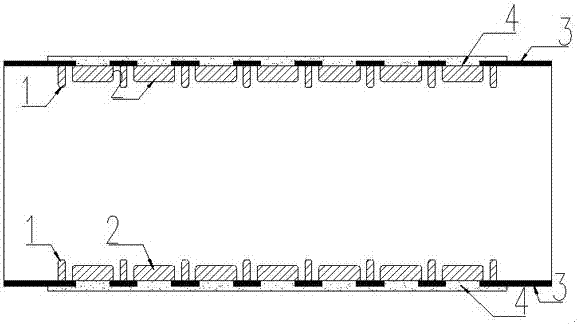
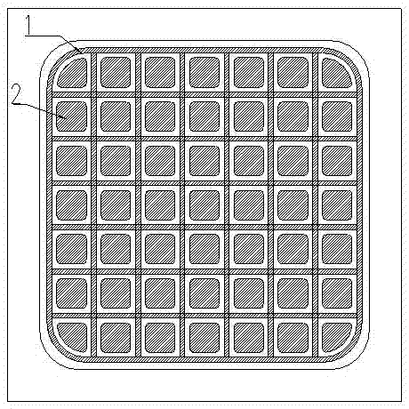
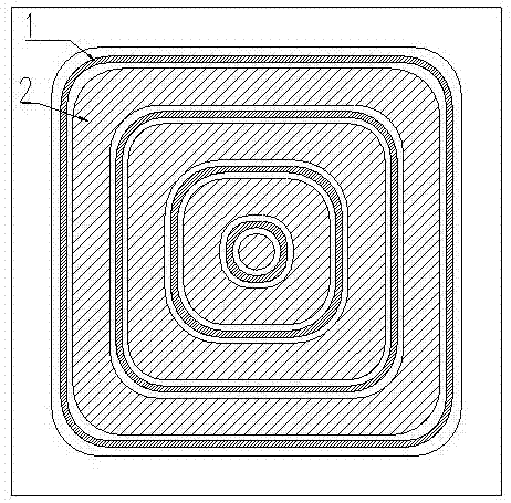
[0035] 4) Double-sided lithography N+ gettering area 1: The longitudinal structure has a short-circuit hole. Using a double-sided lithography machine, align the upper and lower photolithography plates, and place the silicon wafer in the middle of the two photolithography plates. Simultaneous exposure; th...


PUM


Abstract

The invention discloses a low-voltage TVS device with an ultralow electric leakage level and a manufacturing method thereof. The N+ breakdown region (1) and the N+ gettering region (2) of the longitudinal structure can use a vertical crossed structure or a circular annluar structure. The N+ gettering region (1) has a junction depth of 15 to 25 [mu]m and a width range of 20 to 50 [mu]m. The N+ breakdown region (2) has a junction depth of 8 to 15 [mu]m and a width range customized according to different IPP requirements. The N+ gettering region and the N+ breakdown region have gap design requirements of 5 to 50 [mu]m. The main purpose of the N+ gettering region is to absorb oxidation-induced defects generated in the high temperature process of silicon single crystal, and generate a severe defect region. The N + breakdown region is actually the effective working region of the device. The low-voltage TVS device achieves alow electric leakage level and satisfies a requirement for a high IPP current-through capability.

Description

technical field [0001] The invention relates to the technical field of semiconductor chips, in particular to a method for manufacturing a low-voltage TVS device with an ultra-low leakage level. Background technique [0002] Transient suppression diode TVS products are widely used in applications such as solar inverters, set-top boxes, MOSFET protection, industrial controls, telecom base stations, and Power over Ethernet (PoE). In recent years, more and more fields have put forward the demand V BR below 10V, meanwhile, the leakage current I R It is hoped that the lower the value, the better, which will affect the switching response speed and reliability of the device. [0003] The existing technology in China produces TVS devices. Generally, a deep and large-area N+ junction is formed by diffusion on a P-type silicon wafer with a lower resistivity, and is isolated by trenching. By adjusting the junction depth and doping concentration to adjust the voltage. However, for lo...

Claims


Application Information

Patent Timeline
Patent Type & Authority Applications(China)
IPC IPC(8): H01L29/861H01L29/06H01L21/329
CPCH01L29/0603H01L29/0684H01L29/66204H01L29/861Y02P70/50
Inventor 王志超张慧玲朱明
Owner 捷捷半导体有限公司
Why Eureka
Try Eureka