Anti-oxidative processed substrate used for LED packaging and surface processing method thereof

A technology of LED packaging and surface treatment, applied in the secondary treatment of printed circuits, electrical components, circuits, etc., can solve the problems of high process energy consumption, high product cost, large environmental pollution, etc., to achieve a simple production process and great protection significance. , the effect of low material cost

Pending Publication Date: 2017-11-07
HARVATEK OPTOELECTRONICS SHENZHEN
View PDF5 Cites 0 Cited by
  • Summary
  • Abstract
  • Description
  • Claims
  • Application Information

AI Technical Summary

Problems solved by technology

[0004] 1. Gold, silver and other metals are very expensive, resulting in very high product costs;
[0005] 2. The substrate takes a long time in the electroplating process, the production efficiency is not high, and the energy consumption of the whole process is extremely high;
[0006] 3. The wastewater produced by electroplating is more polluting to the environment

Method used


Image

  • Anti-oxidative processed substrate used for LED packaging and surface processing method thereof
  • Anti-oxidative processed substrate used for LED packaging and surface processing method thereof
  • Anti-oxidative processed substrate used for LED packaging and surface processing method thereof

Examples


Embodiment Construction

[0024] The preferred embodiments of the present invention will be described in detail below in conjunction with the accompanying drawings, so that the advantages and features of the present invention can be more easily understood by those skilled in the art, so as to define the protection scope of the present invention more clearly.

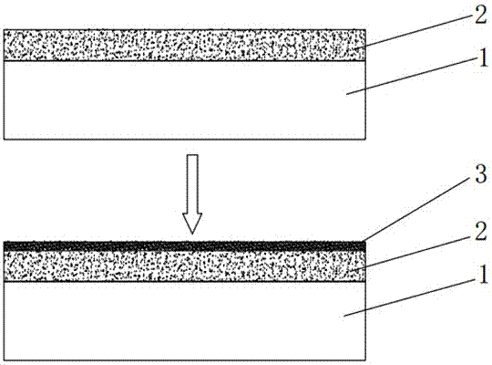
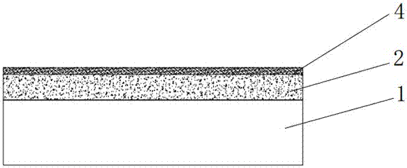
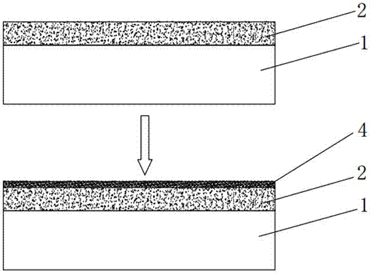
[0025] Please refer to the attached figure 2 , a substrate for LED packaging with anti-oxidation treatment, the PCB substrate includes a resin substrate 1, a layer of copper foil layer 2 is plated on the surface of the resin substrate 1 to be etched, and an organic resin layer is sprayed on the upper surface of the copper foil layer 2 4. The organic resin layer 4 is prepared by mixing the following raw materials by mass:

[0026] Methyltrichlorosilane 10~20%;

[0027] Dimethyldichlorosilane 30~60%;

[0028] Methylphenyl dichlorosilane 10~20%.

[0029] The organic resin layer 4 is an OSP anti-oxidation treated organic resin layer.

[0030] Su...


PUM


Abstract

The invention discloses an anti-oxidative processed substrate used for LED packaging and a surface processing method thereof. A PCB substrate comprises a resin substrate. A surface of the resin substrate, which needs to be etched, is plated with one copper foil layer. One organic resin layer is sprayed on an upper surface of the copper foil layer. The organic resin layer comprises, by weight, 10-20% of methyl trichlorosilane, 30-60% of dimethyl dichlorosilane and 10-20% of methyl-phenyl dichlorosilane. A substrate protection layer adopts an organic protection film. Compared to traditional protection technologies of gold plating, silver plating, nickel plating and the like, the technology in the invention has advantages that material cost is low; a production technology is simple; and a consumed man-hour is greatly shortened compared to that of a traditional electroplating technology. Compared to the traditional electroplating technology, because the surface is sprayed with the organic protection film, the technology has advantages that the material is environmental protection; and sewage generated because of electroplating is greatly reduced, which has a great meaning for environment protection.

Description

technical field [0001] The invention relates to an LED encapsulation process, in particular to an anti-oxidation treated LED encapsulation substrate and a surface treatment method thereof. Background technique [0002] The substrates used for CHIP LED packaging are all copper foil at this stage, and the surface of the copper foil is easy to oxidize. At the same time, in order to facilitate wire bonding, the surface of the copper foil of the substrate needs to be electroplated, such as gold-plated, silver-plated, nickel-plated, etc., so as to protect the copper. The foil is not easy to be oxidized by air, and at the same time, it is easy to solder wires. When customers use it, the solder feet of the LED are easy to be stained with tin. [0003] The substrate copper foil used for CHIP LED packaging needs electroplating, and the current processes are mainly gold plating, silver plating, nickel plating, etc. The above electroplating processes have the following disadvantages: ...

Claims


Application Information

Patent Timeline
Patent Type & Authority Applications(China)
IPC IPC(8): H01L33/48H05K3/28
CPCH01L33/483H05K3/28H01L2933/0033
Inventor 洪汉忠
Owner HARVATEK OPTOELECTRONICS SHENZHEN
Why Eureka
Try Eureka